1
LTC1562
1562fa
Very Low Noise, Low Distortion
Active RC Quad Universal Filter
Continuous TimeNo Clock
Four 2nd Order Filter Sections, 10kHz to 150kHz
Center Frequency
±0.5% Typical Center Frequency Accuracy
±0.3% Typical Center Frequency Accuracy (A Grade)
Wide Variety of Response Shapes
Lowpass, Bandpass and Highpass Responses
103dB Typical S/N, ±5V Supply (Q = 1)
97dB Typical S/N, Single 5V Supply (Q = 1)
96dB Typical S/(N + THD) at ±5V Supply, 20kHz Input
Rail-to-Rail Input and Output Voltages
DC Accurate to 3mV (Typ)
“Zero-Power” Shutdown Mode
Single or Dual Supply, 5V to 10V Total
Resistor-Programmable f
O
, Q, Gain
The LTC
®
1562 is a low noise, low distortion continuous-time
filter with rail-to-rail inputs and outputs, optimized for a
center frequency (f
O
) of 10kHz to 150kHz. Unlike most
monolithic filters, no clock is needed. Four independent 2nd
order filter blocks can be cascaded in any combination, such
as one 8th order or two 4th order filters. Each block’s
response is programmed with three external resistors for
center frequency, Q and gain, using simple design formulas.
Each 2nd order block provides lowpass and bandpass out-
puts. Highpass response is available if an external capacitor
replaces one of the resistors. Allpass, notch and elliptic
responses can also be realized.
The LTC1562 is designed for applications where dynamic
range is important. For example, by cascading 2nd order
sections in pairs, the user can configure the IC as a dual 4th
order Butterworth lowpass filter with 94dB signal-to-noise
ratio from a single 5V power supply. Low level signals can
exploit the built-in gain capability of the LTC1562. Varying the
gain of a section can achieve a dynamic range as high as
118dB with a ±5V supply.
Other cutoff frequency ranges can be provided upon request.
Please contact LTC Marketing.
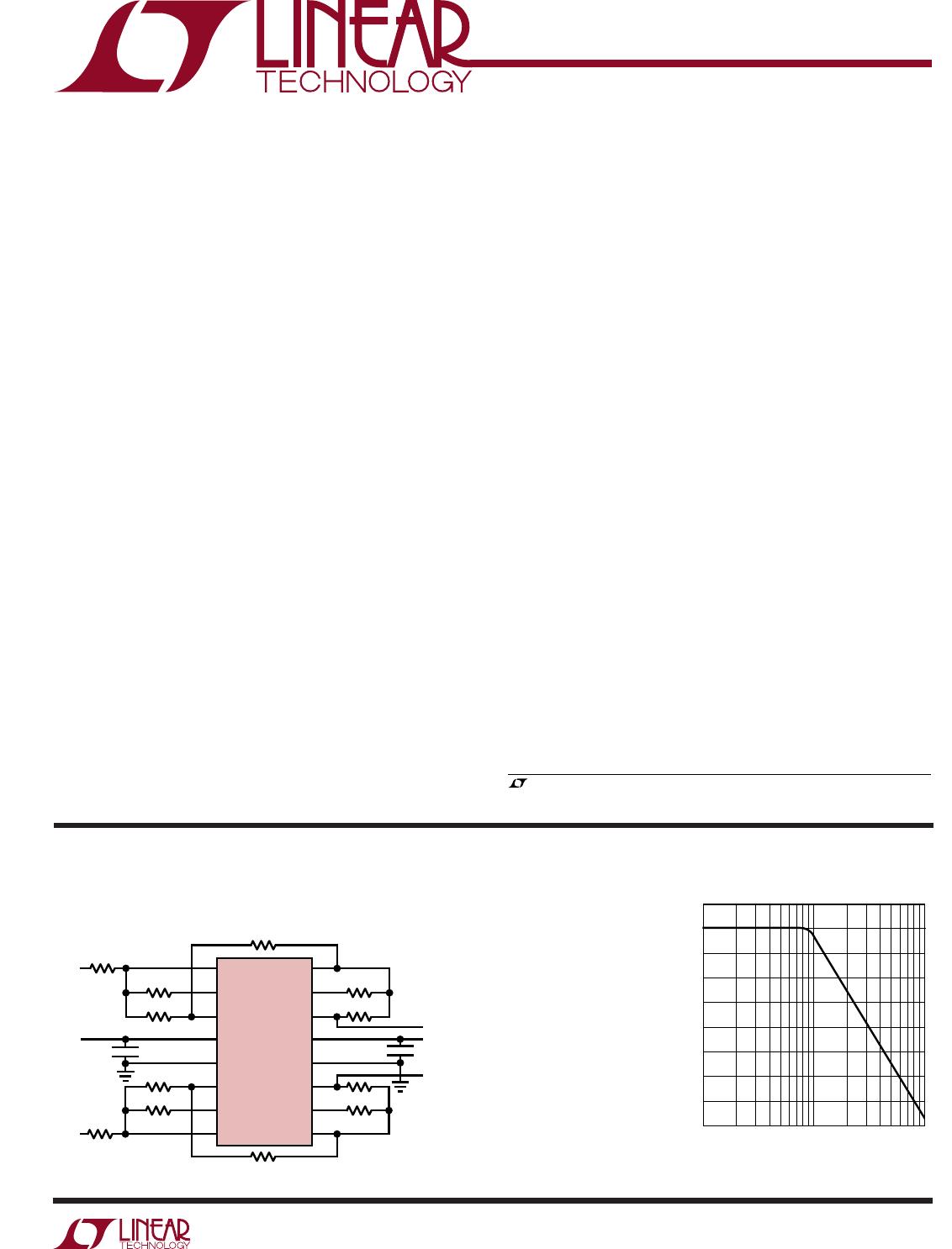
FREQUENCY (Hz)
10k
GAIN (dB)
10
0
–10
–20
–30
–40
–50
–60
–70
–80
100k 1M
1562 TA03b
Amplitude Response
1
2
3
5
6
8
9
10
20
19
18
16
15
13
12
11
INV B
V1 B
V2 B
V
+
SHDN
V2 A
V1 A
INV A
INV C
V1 C
V2 C
V
AGND
V2 D
V1 D
INV D
LTC1562
R
IN2
,
10k
R
IN4
,
10k
R
IN1
10k
V
IN2
V
IN1
SCHEMATIC INCLUDES PIN
NUMBERS FOR 20-PIN PACKAGE.
PINS 4, 7, 14, 17 (NOT SHOWN)
ALSO CONNECT TO V
SEE TYPICAL APPLICATIONS
FOR OTHER CUTOFF FREQUENCIES
DC ACCURATE, NONINVERTING,
UNITY-GAIN, RAIL-TO-RAIL
INPUT AND OUTPUTS. PEAK
SNR 100dB WITH ±5V SUPPLIES
V
OUT1
1562 TA01
V
OUT2
R
IN3
10k
–5V
5V
R
Q1
, 5.62k
R21, 10k
R23, 10k
0.1µF
0.1µF
R
Q3
, 5.62k
R24, 10k
R
Q4
, 13k
R
Q2
, 13k
R22, 10k
Dual 4th Order 100kHz Butterworth Lowpass Filter
High Resolution Systems (14 Bits to 18 Bits)
Antialiasing/Reconstruction Filters
Data Communications, Equalizers
Dual or I-and-Q Channels (Two Matched 4th Order
Filters in One Package)
Linear Phase Filtering
Replacing LC Filter Modules
, LTC and LT are registered trademarks of Linear Technology Corporation.
DESCRIPTIO
U
FEATURES
APPLICATIO S
U
TYPICAL APPLICATIO
U
2
LTC1562
1562fa
PACKAGE/ORDER INFORMATION
W
U
U
ORDER PART
NUMBER
LTC1562CG
LTC1562ACG
LTC1562IG
LTC1562AIG
TOP VIEW
G PACKAGE
20-LEAD PLASTIC SSOP
*G PACKAGE PINS 4, 7, 14, 17 ARE
SUBSTRATE/SHIELD CONNECTIONS
AND MUST BE TIED TO V
1
2
3
4
5
6
7
8
9
10
20
19
18
17
16
15
14
13
12
11
INV B
V1 B
V2 B
V
–*
V
+
SHDN
V
–*
V2 A
V1 A
INV A
INV C
V1 C
V2 C
V
–*
V
AGND
V
–*
V2 D
V1 D
INV D
T
JMAX
= 150°C, θ
JA
= 136°C/W
The denotes the specifications that apply over the full operating
temperature range, otherwise specifications are at T
A
= 25°C. V
S
= ±5V, outputs unloaded, SHDN pin to logic “low”,
unless otherwise noted. AC specs are for a single 2nd order section, R
IN
= R2 = R
Q
=10k ±0.1%, f
O
= 100kHz, unless noted.
SYMBOL PARAMETER CONDITIONS MIN TYP MAX UNITS
V
S
Total Supply Voltage 4.75 10.5 V
I
S
Supply Current V
S
= ±2.375V, R
L
= 5k, C
L
= 30pF, Outputs at 0V 17.3 19.5 mA
V
S
= ±5V, R
L
= 5k, C
L
= 30pF, Outputs at 0V 19 21.5 mA
V
S
= ±2.375V, R
L
= 5k, C
L
= 30pF, Outputs at 0V 23.5 mA
V
S
= ±5V, R
L
= 5k, C
L
= 30pF, Outputs at 0V 25.5 mA
Output Voltage Swing V
S
= ±2.375V, R
L
= 5k, C
L
= 30pF 4.0 4.6 V
P-P
V
S
= ±5V, R
L
= 5k, C
L
= 30pF 9.3 9.8 V
P-P
V
OS
DC Offset Magnitude, V2 Outputs V
S
= ±2.375V, Input at AGND Voltage 315 mV
(Lowpass Response) V
S
= ±5V, Input at AGND Voltage 315 mV
DC AGND Reference Point V
S
= Single 5V Supply 2.5 V
Center Frequency (f
O
) Error (Note 2)
LTC1562 (SSOP) V
S
= ±5V, V2 Output Has R
L
= 5k, C
L
= 30pF 0.5 1.0 %
LTC1562A (SSOP) V
S
= ±5V, V2 Output Has R
L
= 5k, C
L
= 30pF 0.3 0.6 %
LTC1562 (PDIP) V
S
= ±5V, V2 Output Has R
L
= 5k, C
L
= 30pF 0.6 1.5 %
H
L
LP Passband Gain (V2 Output) V
S
= ±2.375V, f
IN
= 10kHz, 0 +0.05 +0.1 dB
V2 Output Has R
L
= 5k, C
L
= 30pF
H
B
BP Passband Gain (V1 Output) V
S
= ±2.375V, f
IN
= f
O
, +0.2 +0.5 dB
V2 Output Has R
L
= 5k, C
L
= 30pF
Total Supply Voltage (V
+
to V
) .............................. 11V
Maximum Input Voltage
at Any Pin ....................(V
– 0.3V) V (V
+
+ 0.3V)
Storage Temperature Range ................. 65°C to 150°C
(Note 1)
Operating Temperature Range
LTC1562C ............................................... 0°C to 70°C
LTC1562I............................................ 40°C to 85°C
Lead Temperature (Soldering, 10 sec).................. 300°C
PACKAGE/ORDER I FOR ATIO
UU
W
ABSOLUTE AXI U RATI GS
WWWU
Consult LTC Marketing for parts specified with wider operating temperature ranges.
ORDER PART
NUMBER
LTC1562CN
1
2
3
4
5
6
7
8
TOP VIEW
N PACKAGE
16-LEAD PDIP
16
15
14
13
12
11
10
9
INV B
V1 B
V2 B
V
+
SHDN
V2 A
V1 A
INV A
INV C
V1 C
V2 C
V
AGND
V2 D
V1 D
INV D
T
JMAX
= 150°C, θ
JA
= 90°C/W
ELECTRICAL CHARACTERISTICS
3
LTC1562
1562fa
SYMBOL PARAMETER CONDITIONS MIN TYP MAX UNITS
Q Error V
S
= ±2.375V, LP Output Has R
L
= 5k, C
L
= 30pF +3 %
Wideband Output Noise, V
S
= ±2.375V, BW = 200kHz, Input AC GND 24 µV
RMS
Lowpass Response (V2 Output) V
S
= ±5V, BW = 200kHz, Input AC GND 24 µV
RMS
Input-Referred Noise, Gain = 100 BW = 200kHz, f
O
= 100kHz, Q = 1, Input AC GND 4.5 µV
RMS
THD Total Harmonic Distortion, f
IN
= 20kHz, 2.8V
P-P
, V1 and V2 Outputs Have 96 dB
Lowpass Response (V2 Output) R
L
= 5k, C
L
= 30pF
f
IN
= 100kHz, 2.8V
P-P
, V1 and V2 Outputs Have 78 dB
R
L
= 5k, C
L
= 30pF
Shutdown Supply Current SHDN Pin to V
+
1.5 15 µA
SHDN Pin to V
+
, V
S
= ±2.375V 1.0 µA
Shutdown-Input Logic Threshold 2.5 V
Shutdown-Input Bias Current SHDN Pin to 0V 10 20 µA
Shutdown Delay SHDN Pin Steps from 0V
to V
+
20 µs
Shutdown Recovery Delay SHDN Pin Steps from V
+
to 0V 100 µs
Inverting Input Bias Current, Each Biquad 5 pA
Note 1: Absolute Maximum Ratings are those values beyond which the life
of a device may be impaired.
TYPICAL PERFOR A CE CHARACTERISTICS
UW
NOMINAL f
O
(kHz)
50
Q ERROR (%)
35
30
25
20
15
10
5
0
–5
130
1562 G03
70 90 110 15012060 80 100 140
T
A
= 70°C
T
A
= 25°C
R
IN
= R
Q
Q = 10
Q = 5
Q = 2.5
Q = 1
Q Error vs Nominal f
O
(V
S
= ±5V)
NOMINAL f
O
(kHz)
50
f
O
ERROR (%)
0
0.50
1.00
0.75
1.50
1.25
130
1562 G01
0.50
1.00
0.25
0.25
0.75
1.25
1.50
70
90
110
150
120
60
80
100
140
Q = 5
Q = 2.5
Q = 1
f
O
Error vs Nominal f
O
(V
S
= ±5V)
NOMINAL f
O
(kHz)
50
f
O
ERROR (%)
0
0.50
1.00
0.75
1.50
1.25
130
1562 G02
0.50
1.00
0.25
0.25
0.75
1.25
1.50
70
90
110
150
120
60
80
100
140
Q = 5
Q = 2.5
Q = 1
f
O
Error vs Nominal f
O
(V
S
= ±2.5V)
The denotes the specifications that apply over the full operating
temperature range, otherwise specifications are at T
A
= 25°C. V
S
= ±5V, outputs unloaded, SHDN pin to logic “low”,
unless otherwise noted. AC specs are for a single 2nd order section, R
IN
= R2 = R
Q
=10k ±0.1%, f
O
= 100kHz, unless noted.
ELECTRICAL CHARACTERISTICS
Note 2: f
O
change from ±5V to ±2.375 supplies is –0.15% typical,
f
O
temperature coefficient, –40°C to 85°C, is –25ppm/°C typical.

LTC1562CN#PBF

Mfr. #:
Manufacturer:
Analog Devices Inc.
Description:
Active Filter Active RC Quad Universal Filter
Lifecycle:
New from this manufacturer.
Delivery:
DHL FedEx Ups TNT EMS
Payment:
T/T Paypal Visa MoneyGram Western Union