17
LTC1562
1562fa
(Basic)
TYPICAL APPLICATIONS
U
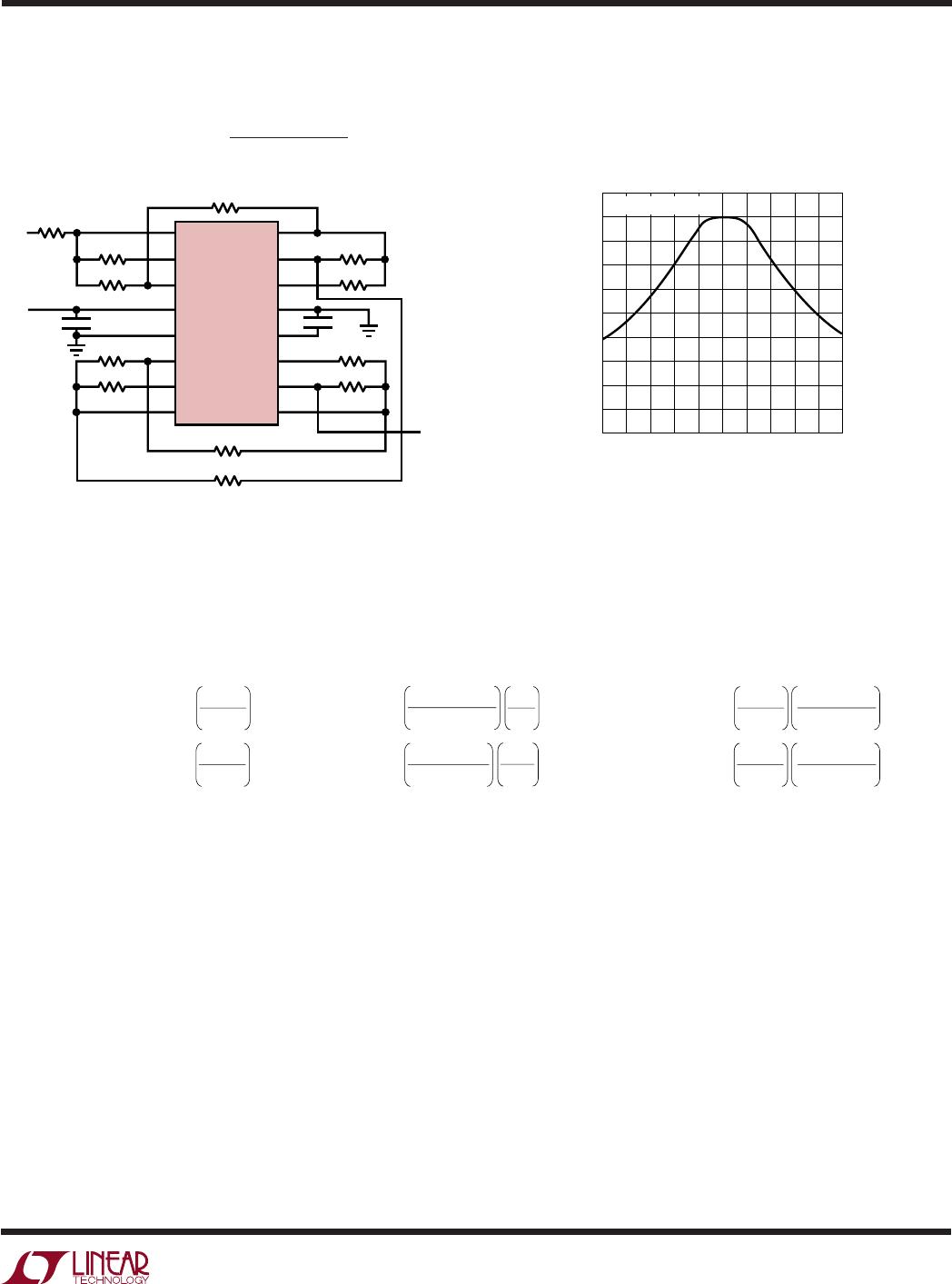
Amplitude Response
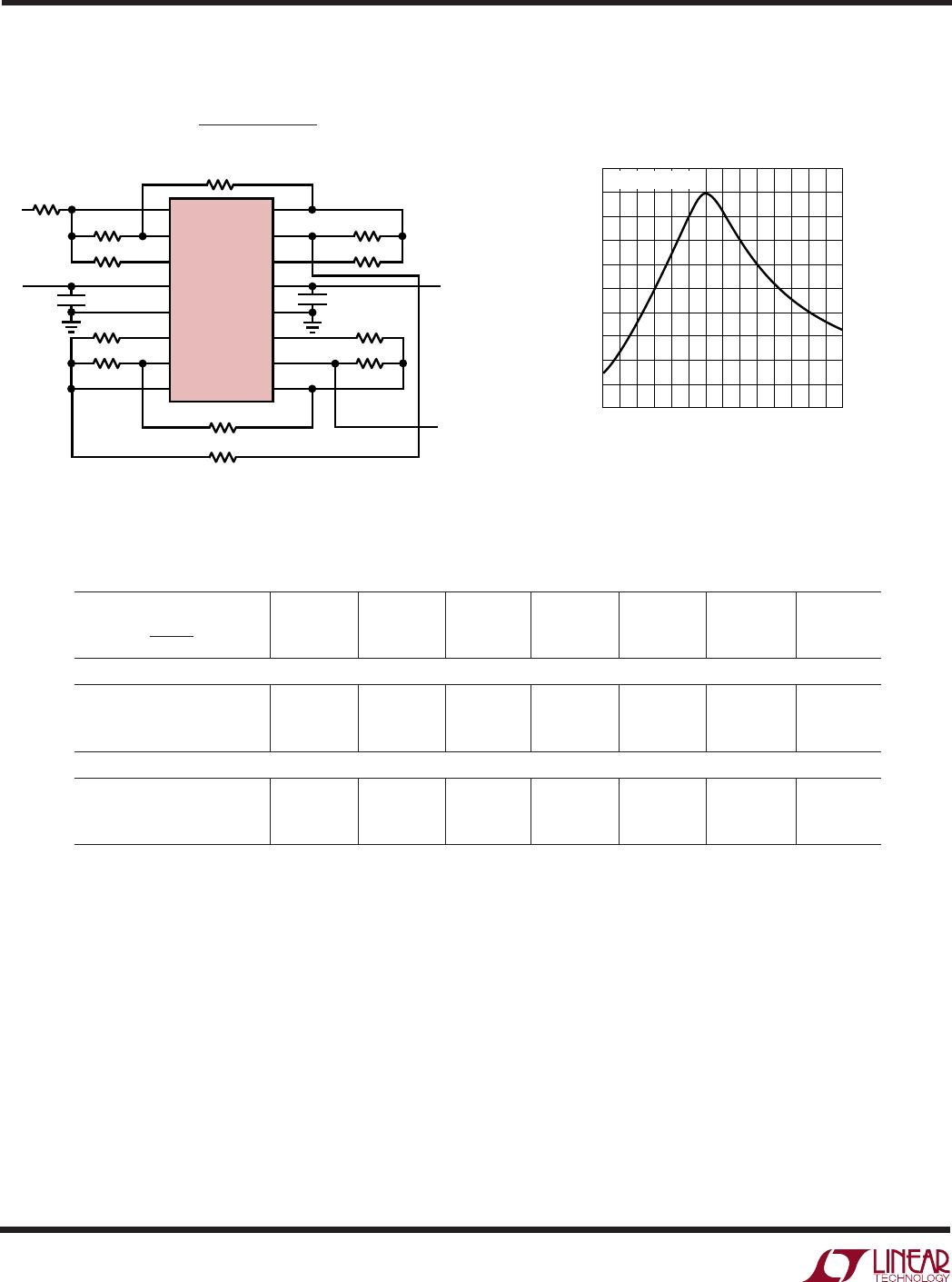
8th Order Bandpass Filter, Single 5V Supply,
–1dB Bandwidth =
Center Frequency
10
FREQUENCY (kHz)
60
GAIN (dB)
–30
–10
10
124
1562 TA06b
–50
–70
–40
–20
0
–60
–80
–90
76
92
108
68 132
84
100
116
140
f
CENTER
= 100kHz
R21 = R23 = 11.7k
Quick Design Formulas for a Center Frequency f
C
(Recommended Range 50kHz to 120kHz):
2
2
100kHz
ƒ
C
R
IN1
= R
IN3
=
R21
2.56
R22 = R24 = 8.66k
100kHz
ƒ
C
ƒ
C
+ 1736kHz
100kHz
R
IN2
= R
IN4
=
R
Q2
14.36
ƒ
C
+ 634kHz
100kHz
Notes: R21 and R
Q2
should be rounded to the nearest standard finite-tolerance value
before
using these values in
the later formulas. For f
C
< 100kHz, the maximum peak-to-peak passband input level is (f
C
/100kHz)5V. Use
LTC1562A for minimum variation of passband gain.
Example: Center frequency f
C
of 100kHz. The formulas give R21 = R23 = 11.7k, nearest standard 1% value 11.5k.
This value gives R
IN1
= R
IN3
= 82.46k, nearest 1% value 82.5k. R
Q1
= R
Q3
= 65.5k, nearest 1% value 64.9k.
R22 = R24 = 8.66k, already a standard 1% value. This gives R
IN2
= R
IN4
= 32.4k (again already a standard 1% value).
R
Q2
= R
Q4
= 63.45k, nearest 1% value 63.4k. If LTC1562A is used, resistor tolerances tighter than 1% will further
improve the passband gain accuracy.
R
Q1
= R
Q3
= 215.5k
100kHz
ƒ
C
100kHz
ƒ
C
1562 TA06 TABLE
100kHz
ƒ
C
+ 229kHz
R
Q2
= R
Q4
= 286.2k
100kHz
ƒ
C
+ 351kHz
1
2
3
5
6
8
9
10
20
19
18
16
15
13
12
11
INV B
V1 B
V2 B
V
+
SHDN
V2 A
V1 A
INV A
INV C
V1 C
V2 C
V
–
AGND
V2 D
V1 D
INV D
LTC1562
R
IN2
R
IN4
R
IN1
V
IN
V
OUT
1562 TA06a
R
IN3
5V
R
Q1
R21
R23
0.1µF
1µF
R
Q3
R24
R
Q4
R
Q2
R22
SCHEMATIC INCLUDES PIN NUMBERS FOR 20-PIN PACKAGE.
PINS 4, 7, 14, 17 (NOT SHOWN) ALSO CONNECT TO V
–