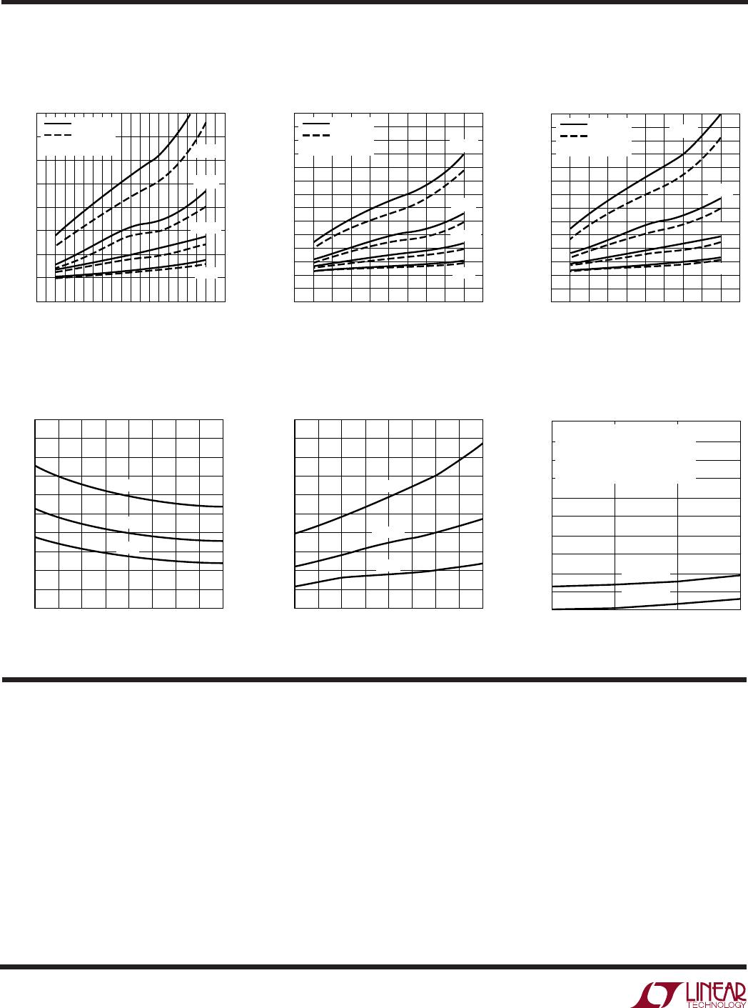
4
LTC1562
1562fa
TYPICAL PERFOR A CE CHARACTERISTICS
UW
Peak BP Gain vs Nominal f
O
(V
S
= ±5V) (Figure 3, V1 Output)Q Error vs Nominal f
O
(V
S
= ±2.5V)
NOMINAL f
O
(kHz)
50
Q ERROR (%)
35
30
25
20
15
10
5
0
–5
130
1562 G04
70 90 110 15012060 80 100 140
Q = 10
Q = 5
Q = 2.5
Q = 1
T
A
= 70°C
T
A
= 25°C
R
IN
= R
Q
NOMINAL f
O
(kHz)
50
0.5
PEAK BP GAIN (dB)
0
0.5
1.0
3.0
2.0
70
90
100 140
2.5
1.5
60 80
110
120
130
150
1562 G5
Q = 10
Q = 5
Q = 2.5
Q = 1
T
A
= 70°C
T
A
= 25°C
R
IN
= R
Q
NOMINAL f
O
(kHz)
50
0.5
PEAK BP GAIN (dB)
0
0.5
1.0
3.0
2.0
70
90
100 140
2.5
1.5
60 80
110
120
130
150
1562 G6
Q = 10
Q = 5
Q = 2.5
Q = 1
T
A
= 70°C
T
A
= 25°C
R
IN
= R
Q
Peak BP Gain vs Nominal f
O
(V
S
= ±2.5V) (Figure 3, V1 Output)
Distortion vs External Load
Resistance (V
S
= ±5V, 25°C)
(Figure 8)
EXTERNAL LOAD RESISTANCE ()
10k
–100
THD (AMPLITUDE BELOW FUNDAMENTAL) (dB)
–80
–70
–60
–50
–40
–30
5k
2k
1562 G09
–20
–10
0
–90
1k
f
IN
= 50kHz
f
IN
= 20kHz
2nd ORDER LOWPASS
f
O
= 100kHz
Q = 0.7
OUTPUT LEVEL 1V
RMS
(2.83V
P-P
)
±5V SUPPLIES
LP Noise vs Nominal f
O
(V
S
= ±5V, 25°C) (Figure 3,
V2 Output) (R
IN
= R2)
NOMINAL f
O
(kHz)
60
10
BP NOISE (µV
RMS
)
15
25
30
35
60
45
80
100
110
1562 G08
20
50
55
40
70 90
120
130
140
Q = 5
Q = 2.5
Q = 1
Power Supply Pins: The V
+
and V
pins should be
bypassed with 0.1µF capacitors to an adequate analog
ground or ground plane. These capacitors should be
connected as closely as possible to the supply pins. In the
20-lead SSOP package, the additional pins 4, 7, 14 and 17
are internally connected to V
(Pin 16) and should also be
tied to the same point as Pin 16 for best shielding. Low
noise linear supplies are recommended. Switching sup-
plies are not recommended as they will lower the filter
dynamic range.
Analog Ground (AGND): The AGND pin is the midpoint of
an internal resistive voltage divider, developing a potential
halfway between the V
+
and V
pins, with an equivalent
series resistance nominally 7k. This serves as an inter-
nal ground reference. Filter performance will reflect the
quality of the analog signal ground and an analog ground
plane surrounding the package is recommended. The
analog ground plane should be connected to any digital
ground at a single point. For dual supply operation, the
AGND pin should be connected to the ground plane
BP Noise vs Nominal f
O
(V
S
= ±5V, 25°C) (Figure 3,
V1 Output) (R
IN
= R
Q
)
NOMINAL f
O
(kHz)
60
10
NOISE (µV
RMS
)
15
25
30
35
60
45
80
100
110
1562 G07
20
50
55
40
70 90
120
130
140
Q = 5
Q = 2.5
Q = 1
UU
U
PI FU CTIO S
5
LTC1562
1562fa
PIN FUNCTIONS
UUU
package does not have the four substrate pins (Pins 4, 7,
14, 17 in the 20-pin package).
Shutdown (SHDN): When the SHDN input goes high or is
open-circuited, the LTC1562 enters a “zero-power” shut-
down state and only junction leakage currents flow. The
AGND pin and the amplifier outputs (see Figure 3) assume
a high impedance state and the amplifiers effectively
disappear from the circuit. (If an input signal is applied to
a complete filter circuit while the LTC1562 is in shutdown,
some signal will normally flow to the output through
passive components around the inactive op amps.)
A small pull-up current source at the SHDN input
defaults
the LTC1562 to the shutdown state if the SHDN pin is left
floating
. Therefore, the user
must
connect the SHDN pin
to a logic “low” (0V for ±5V supplies, V
for 5V total
supply) for normal operation of the LTC1562. (This con-
vention permits true “zero-power” shutdown since not
even the driving logic must deliver current while the part
is in shutdown.) With a single supply voltage, use V
for
logic “low”—do not connect SHDN to the AGND pin.
(Figure 1). For single supply operation, the AGND pin
should be bypassed to the ground plane with at least a
0.1µF capacitor (at least 1µF for best AC performance)
(Figure 2). These figures show 20-pin package connec-
tions. The same principles apply to the 16-pin package
with allowance for its different pin numbers. The 16-pin
Figure 1. Dual Supply Ground Plane Connection
(Including Substrate Pins 4, 7, 14, 17)
0.1µF
V
1562 F01
DIGITAL
GROUND PLANE
(IF ANY)
V
+
LTC1562
20-PIN SSOP
0.1µF
ANALOG
GROUND
PLANE
20
19
18
17
16
15
14
13
12
11
1
2
3
4
5
6
7
8
9
10
SINGLE-POINT
SYSTEM GROUND
1µF
1562 F01
DIGITAL
GROUND PLANE
(IF ANY)
V
+
LTC1562
20-PIN SSOP
V
+
/2
REFERENCE
0.1µF
ANALOG
GROUND
PLANE
20
19
18
17
16
15
14
13
12
11
1
2
3
4
5
6
7
8
9
10
SINGLE-POINT
SYSTEM GROUND
Figure 2. Single Supply Ground Plane Connection
(Including Substrate Pins 4, 7, 14, 17)
+
+
R2
R
Q
V
IN
INV
*R1 AND C ARE PRECISION
INTERNAL COMPONENTS
V2 V1
1/4 LTC1562
1562 F01
C
1
sR1C*
Z
IN
Z
IN
TYPE
R
C
RESPONSE
AT V1
BANDPASS
HIGHPASS
RESPONSE
AT V2
LOWPASS
BANDPASS
10k
R2
IN EACH CASE,
Q =
f
O
= (100kHz)
RQ
R2
()
100kHz
f
O
()
Figure 3. Equivalent Circuit of a Single 2nd Order Section
(Inside Dashed Line) Shown in Typical Connection. Form of Z
IN
Determines Response Types at the Two Outputs (See Table)
6
LTC1562
1562fa
PIN FUNCTIONS
UUU
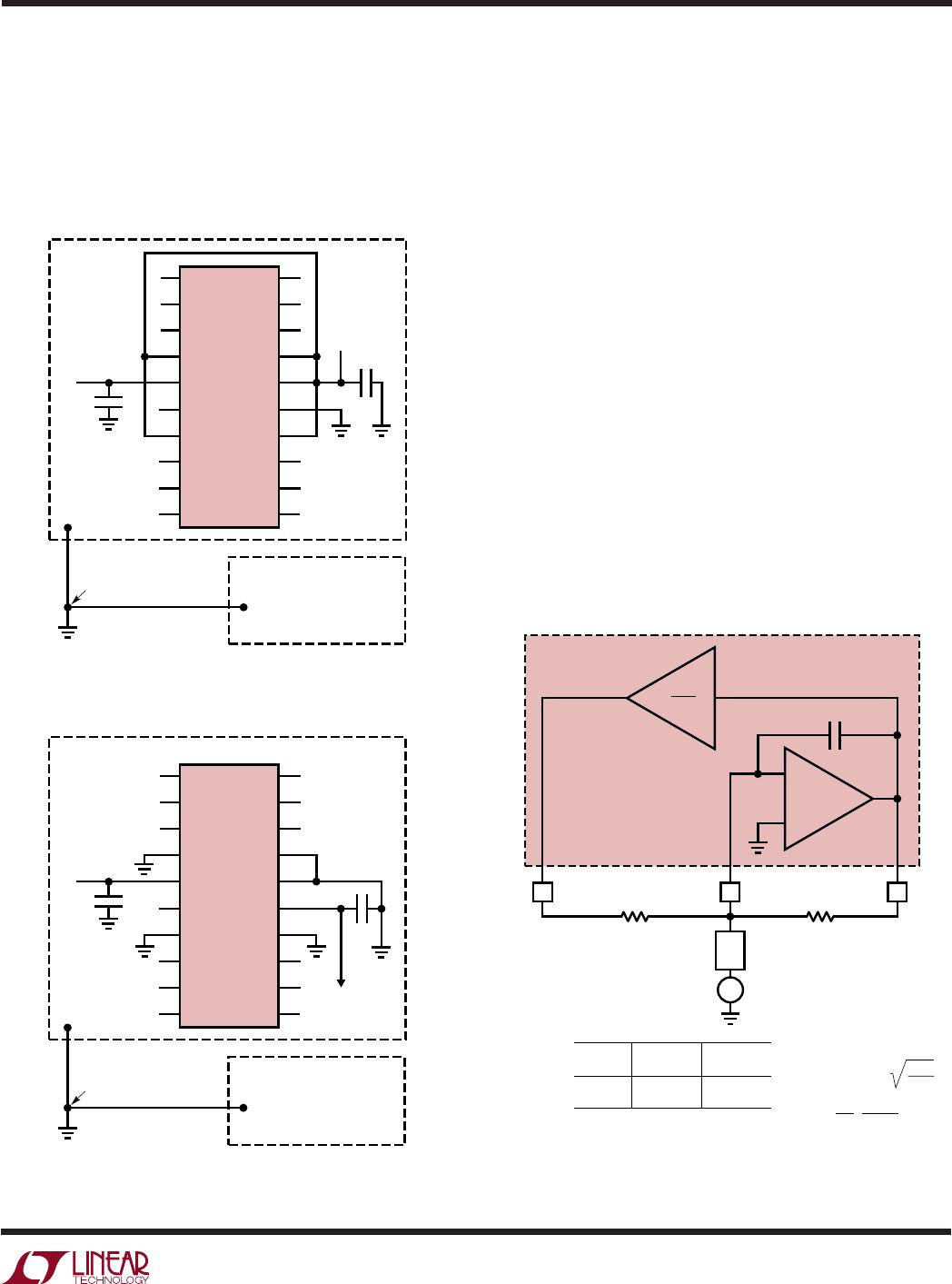
INV A, INV B, INV C, INV D: Each of the INV pins is a virtual-
ground summing point for the corresponding 2nd order
section. For each section, external components Z
IN
, R2,
R
Q
connect to the INV pin as shown in Figure 3 and
described further in the Applications Information. Note
that the INV pins are sensitive internal nodes of the filter
and will readily receive any unintended signals that are
capacitively coupled into them. Capacitance to the INV
nodes will also affect the frequency response of the filter
sections. For these reasons, printed circuit connections to
the INV pins must be kept as short as possible, less than
one inch (2.5cm) total and surrounded by a ground plane.
V1 A, V1 B, V1 C, V1 D: Output Pins. Provide a bandpass,
highpass or other response depending on external cir-
cuitry (see Applications Information section). Each V1 pin
also connects to the R
Q
resistor of the corresponding 2nd
order filter section (see Figure 3 and Applications Informa-
tion). Each output is designed to drive a nominal net load
of 5k and 30pF, which includes the loading due to the
external R
Q
. Distortion performance improves when the
outputs are loaded as lightly as possible. Some earlier
literature refers to these outputs as “BP” rather than V1.
V2 A, V2 B, V2 C, V2 D: Output Pins. Provide a lowpass,
bandpass or other response depending on external cir-
cuitry (see Applications Information section). Each V2 pin
also connects to the R2 resistor of the corresponding 2nd
order filter section (see Figure 3 and Applications Informa-
tion). Each output is designed to drive a nominal net load
of 5k and 30pF, which includes the loading due to the
external R2. Distortion performance improves when the
outputs are loaded as lightly as possible. Some earlier
literature refers to these outputs as “LP” rather than V2.
BLOCK DIAGRA
W
Overall Block Diagram Showing Four 3-Terminal 2nd Order Sections
V
+
V
SHDN
1562 BD
2ND ORDER SECTIONS
R
R
INV V1 V2
C
SHUTDOWN
SWITCH
SHUTDOWN
SWITCH
AGND
V
+
V
+
INV V1 V2
INV V1 V2 INV V1 V2
C
CC
AB
DC
+
+
+
∫∫
∫∫

LTC1562CN#PBF

Mfr. #:
Manufacturer:
Analog Devices Inc.
Description:
Active Filter Active RC Quad Universal Filter
Lifecycle:
New from this manufacturer.
Delivery:
DHL FedEx Ups TNT EMS
Payment:
T/T Paypal Visa MoneyGram Western Union