19
LTC1562
1562fa
(Basic)
TYPICAL APPLICATIONS
U
Amplitude Response
1
2
3
5
6
8
9
10
20
19
18
16
15
13
12
11
INV B
V1 B
V2 B
V
+
SHDN
V2 A
V1 A
INV A
INV C
V1 C
V2 C
V
AGND
V2 D
V1 D
INV D
LTC1562
R
IN2
,
5.23k
R
IN4
,
3.4k
C
IN1
150pF
V
IN
V
OUT
1562 TA11a
R
IN3
, 8.06k
5V –5V
R
Q1
, 30.1k
R21, 110k
R23, 5.23k
0.1µF
0.1µF
R
Q3
, 14k
R24, 5.23k
R
Q4
, 3.74k
R
Q2
, 5.11k
R22, 5.23k
SCHEMATIC INCLUDES PIN NUMBERS FOR 20-PIN PACKAGE.
PINS 4, 7, 14, 17 (NOT SHOWN) ALSO CONNECT TO V
ALL RESISTORS = 1% METAL FILM
2nd Order 30kHz Highpass Cascaded with 6th Order 138kHz Lowpass
8th Order Wideband Bandpass Filter
f
CENTER
= 50kHz, –3dB BW 40kHz to 60kHz
1
2
3
5
6
8
9
10
20
19
18
16
15
13
12
11
INV B
V1 B
V2 B
V
+
SHDN
V2 A
V1 A
INV A
INV C
V1 C
V2 C
V
AGND
V2 D
V1 D
INV D
LTC1562
C
IN1
22pF
V
IN
V
OUT
1562 TA09a
V
+
V
R
Q1
59k
R21 56.2k
R
IN2
69.8k
R23 63.4k
0.1µF
1µF
R
Q3
82.5k
R24 28.7k
R
Q4
100k
R
Q2
48.7k
R22 34.8k
C
IN4
47pF
C
IN3
27pF
SCHEMATIC INCLUDES PIN NUMBERS FOR 20-PIN PACKAGE.
PINS 4, 7, 14, 17 (NOT SHOWN) ALSO CONNECT TO V
FREQUENCY (kHz)
–60
–30
–40
–50
10
0
–10
–20
1562 TA09b
GAIN (dB)
20
100
Amplitude Response
FREQUENCY (kHz)
10
GAIN (dB)
20
10
0
–10
–20
–30
–40
–50
–60
–70
–80
100 400
1562 TA11b
8th Order Highpass 0.05dB Ripple Chebyshev Filter f
CUTOFF
= 30kHz
1
2
3
5
6
8
9
10
20
19
18
16
15
13
12
11
INV B
V1 B
V2 B
V
+
SHDN
V2 A
V1 A
INV A
INV C
V1 C
V2 C
V
AGND
V2 D
V1 D
INV D
LTC1562
C
IN1
150pF
C
IN
1562 TA10a
V
OUT
–5V
5V
R
Q1
, 10.2k
R21, 35.7k
R23, 107k
0.1µF
0.1µF
R
Q3
, 54.9k
R24, 127k
R
Q4
, 98.9k
R
Q2
, 22.1k
R22, 66.5k
C
IN3
150pF
C
IN4
150pF
C
IN2
150pF
SCHEMATIC INCLUDES PIN NUMBERS FOR 20-PIN PACKAGE.
PINS 4, 7, 14, 17 (NOT SHOWN) ALSO CONNECT TO V
TOTAL OUTPUT NOISE = 40µV
RMS
Amplitude Response
FREQUENCY (Hz)
1k
GAIN (dB)
10
0
–10
–20
–30
–40
–50
–60
–70
–80
–90
10k 100k 1M
1562 TA10b
20
LTC1562
1562fa
APPLICATIONS INFORMATION
WUU
U
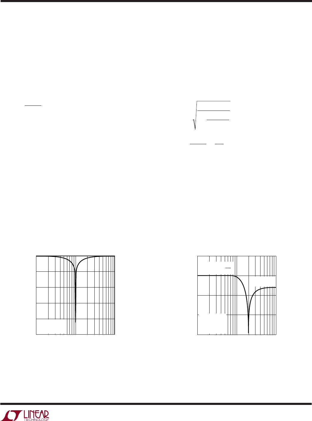
Notches and Elliptic Responses
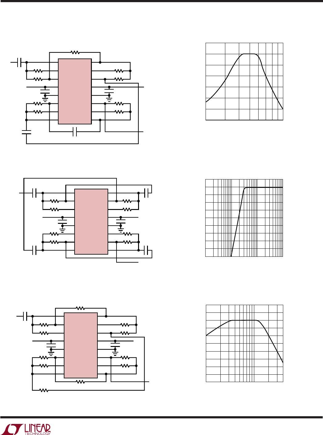
The basic (essentially all-pole) LTC1562 circuit tech-
niques described so far will serve many applications.
However, the sharpest-cutoff lowpass, highpass and band-
pass filters include notches (imaginary zero pairs) in the
stopbands. A notch, or band-reject, filter has zero gain at
a frequency f
N
. Notches are also occasionally used by
themselves to reject a narrow band of frequencies. A
number of circuit methods will give notch responses from
an Operational Filter block. Each method exhibits an input-
output transfer function that is a standard 2nd order band-
reject response:
Hs
Hs
sQs
BR
N
N
O
O
()
/
=
+
()
+
()
+
22
22
ω
ωω
with parameters ω
N
= 2πf
N
and H
N
set by component
values as described below. (ω
0
= 2πf
0
and Q are set for the
Operational Filter block by its R2 and R
Q
resistors as
described earlier in Setting f
0
and Q). Characteristically,
the gain magnitude |H
BR
(j2πf)| has the value H
N
(f
N
2
/f
0
2
) at
DC (f = 0) and H
N
at high frequencies (f >> f
N
), so in
addition to the notch, the gain changes by a factor:
HighFrequency Gain
DC Gain
O
N
=
ƒ
ƒ
2
2
The common principle in the following circuit methods is
to add a signal to a filtered replica of itself having equal gain
and 180° phase difference at the desired notch frequency
f
N
. The two signals then cancel out at frequency f
N
. The
notch depth (the completeness of cancellation) will be
infinite to the extent that the two paths have matching
gains. Three practical circuit methods are presented here,
with different features and advantages.
Examples and design procedures for practical filters using
these techniques appear in a series of articles attached to
this data sheet on the Linear Technology web site
(www.linear-tech.com). Also available free is the analog
filter design software, FilterCAD for Windows, recom-
mended for designing filters not shown in the Typical
Applications schematics in this data sheet.
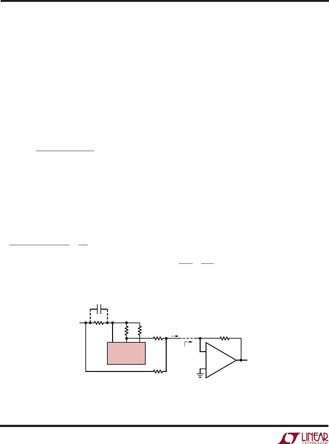
Elementary Feedforward Notches
A “textbook” method to get a 180° phase difference at
frequency f
N
for a notch is to dedicate a bandpass 2nd
order section (described earlier under Basic Bandpass),
which gives 180° phase shift at the section’s center
frequency f
O
(Figure 11, with C
IN1
= 0), so that f
N
= f
O
. The
bandpass section of Figure 6a, at its center frequency f
O
,
has a phase shift of 180° and a gain magnitude of H
B
=
R
Q
/R
IN
. A notch results in Figure 11 if the paths summed
into virtual ground have the same gains at the 180°
frequency (then I
O
= 0). This requires a constraint on the
resistor values:
R
R
R
R
IN
FF
Q
IN
2
2
1
1
=
INV V1
2nd ORDER
1/4 LTC1562
V2
R21R
Q1
R
IN1
R
IN2
R
GAIN
I
O
R
FF2
C
IN1
V
IN
V
OUT
1562 F11
VIRTUAL
GROUND
+
Figure 11. Feedforward Notch Configuration for f
N
f
O
21
LTC1562
1562fa
APPLICATIONS INFORMATION
WUU
U
Note that the depth of the notch depends on the accuracy
of this resistor ratioing. The virtual-ground summing
point in Figure 11 may be from an op amp as shown, or in
a practical cascaded filter, the INV input of another Opera-
tional Filter block. The transfer function in Figure 11 with
C
IN1
= 0 is a “pure” notch (f
N
= f
0
) of the H
BR
(s) form above,
and the parameters are:
ƒ=ƒ
=
NO
N
GAIN
FF
H
R
R
2
Because f
N
= f
0
in this case, the gain magnitude both at DC
and at high frequencies (f >> f
N
) is the same, H
N
(assuming
that the op amp in Figure 11 adds no significant frequency
response). Figure 12 shows this. Such a notch is ineffi-
cient as a cascaded part of a highpass, lowpass or band-
pass filter (the most common uses for notches). Varia-
tions of Figure 11 can add a highpass or lowpass shape to
the notch, without using more Operational Filter blocks.
The key to doing so is to decouple the notch frequency f
N
from the center frequency f
0
of the Operational Filter block
(this is shown in Figures 13 and 15). The next two sections
summarize two variations of Figure 11 with this highpass/
lowpass shaping, and the remaining section shows a
different approach to building notches.
Feedforward Notches for f
N
> f
0
When C
IN1
0 in Figure 11, the notch frequency f
N
is above
the center frequency f
0
and the response has a lowpass
shape as well as a notch (Figure 13). C
IN1
contributes
phase lead, which increases the notch frequency above
the center frequency of the 2nd order Operational Filter
block. The resistor constraint from the previous section
also applies here and the H
BR
(s) parameters become:
C is the internal capacitor value in the Operational Filter
block (in the LTC1562, 159pF).
The configuration of Figure 11 is most useful for a
stopband notch in a lowpass filter or as an upper stopband
notch in a bandpass filter, since the two resistors R
IN2
and
R
FF2
can replace the input resistor R
IN
of either a lowpass
section (Figure 5) or a resistor-input bandpass section
(Figure 6a) built from a second Operational Filter block.
Figure 12. Notch Response with f
N
= f
O
FREQUENCY (kHz)
10
–60
GAIN (dB)
–40
–20
20
100 1000
1562 F13
0
f
O
= 100kHz
f
N
= 200kHz
Q = 1
DC GAIN = 0dB
f
N
2
f
O
2
DC GAIN = H
N
()
HIGH FREQ
GAIN = H
N
FREQUENCY (kHz)
10
100
GAIN (dB)
–40
–20
0
100 1000
AN54 • TA18
–60
–80
f
N
= f
O
= 100kHz
H
N
= 1
Q = 1
Figure 13. Notch Response with f
N
> f
O

LTC1562CN#PBF

Mfr. #:
Manufacturer:
Analog Devices Inc.
Description:
Active Filter Active RC Quad Universal Filter
Lifecycle:
New from this manufacturer.
Delivery:
DHL FedEx Ups TNT EMS
Payment:
T/T Paypal Visa MoneyGram Western Union