1
©2009 Integrated Device Technology, Inc. All rights reserved. Product specifications subject to change without notice. DSC-5941/10
FEBRUARY 2009
3.3V MULTI-QUEUE FLOW-CONTROL DEVICES
(4 QUEUES) 18 BIT WIDE CONFIGURATION
589,824 bits
1,179,648 bits
2,359,296 bits
IDT and the IDT logo are registered trademarks of Integrated Device Technology, Inc.
COMMERCIAL AND INDUSTRIAL TEMPERATURE RANGES
IDT72V51233
IDT72V51243
IDT72V51253
FEATURES:
Choose from among the following memory density options:
IDT72V51233
Total Available Memory = 589,824 bits
IDT72V51243
Total Available Memory = 1,179,648 bits
IDT72V51253
Total Available Memory = 2,359,296 bits
Configurable from 1 to 4 Queues
Queues may be configured at master reset from the pool of
Total Available Memory in blocks of 512 x 18 or 1,024 x 9
Independent Read and Write access per queue
User programmable via serial port
Default multi-queue device configurations
-IDT72V51233: 8,192 x 18 x 4Q or 16,384 x 9 x 4Q
-IDT72V51243: 16,384 x 18 x 4Q or 32,768 x 9 x 4Q
-IDT72V51253: 32,768 x 18 x 4Q or 65,536 x 9 x 4Q
100% Bus Utilization, Read and Write on every clock cycle
166 MHz High speed operation (6ns cycle time)
3.7ns access time
Individual, Active queue flags (OV, FF, PAE, PAF)
4 bit parallel flag status on both read and write ports
Provides continuous PAE and PAF status of up to 4 Queues
Global Bus Matching - (All Queues have same Input Bus Width
and Output Bus Width)
User Selectable Bus Matching Options:
- x18in to x18out
- x9in to x18out
- x18in to x9out
- x9in to x9out
FWFT mode of operation on read port
Partial Reset, clears data in single Queue
Expansion of up to 8 multi-queue devices in parallel is available
JTAG Functionality (Boundary Scan)
Available in a 256-pin PBGA, 1mm pitch, 17mm x 17mm
HIGH Performance submicron CMOS technology
Industrial temperature range (-40°C to +85°C) is available
Q
0
Q
3
MULTI-QUEUE FLOW-CONTROL DEVICE
FSTR
WEN
PAF
FF
WRADD
5
WCLK
PAFn
x9, x18
DATA IN
REN
PAE
RDADD
ESTR
RCLK
PAEn
x9, x18
DATA OUT
OE
OV
WRITE CONTROL
D
in
Q
out
4
4
6
READ CONTROL
WRITE FLAGS
READ FLAGS
5941 drw01
WADEN
RADEN
FUNCTIONAL BLOCK DIAGRAM
2
COMMERCIAL AND INDUSTRIAL
TEMPERATURE RANGES
IDT72V51233/72V51243/72V51253 3.3V, MULTI-QUEUE FLOW-CONTROL DEVICES
(4 QUEUES) 18 BIT WIDE CONFIGURATION 589,824, 1,179,648 and 2,359,296 bits
DESCRIPTION:
The IDT72V51233/72V51243/72V51253 multi-queue flow-control de-
vices are single chip within which anywhere between 1 and 4 discrete FIFO
queues can be setup. All queues within the device have a common data input
bus, (write port) and a common data output bus, (read port). Data written into
the write port is directed to a respective queue via an internal de-multiplex
operation, addressed by the user. Data read from the read port is accessed
from a respective queue via an internal multiplex operation, addressed by
the user. Data writes and reads can be performed at high speeds up to
166MHz, with access times of 3.7ns. Data write and read operations are totally
independent of each other, a queue maybe selected on the write port and
a different queue on the read port or both ports may select the same queue
simultaneously.
The device provides Full flag and Output Valid flag status for the queue
selected for write and read operations respectively. Also a Programmable
Almost Full and Programmable Almost Empty flag for each queue is provided.
Two 4 bit programmable flag busses are available, providing status of all
queues, including queues not selected for write or read operations, these flag
busses provide an individual flag per queue.
Bus Matching is available on this device, either port can be 9 bits or 18 bits
wide. When Bus Matching is used the device ensures the logical transfer of data
throughput in a Little Endian manner.
The user has full flexibility configuring queues within the device, being able
to program the total number of queues between 1 and 4, the individual queue
depths being independent of each other. The programmable flag positions are
also user programmable. All programming is done via a dedicated serial port.
If the user does not wish to program the multi-queue device, a default option is
available that configures the device in a predetermined manner.
Both Master Reset and Partial Reset pins are provided on this device. A Master
Reset latches in all configuration setup pins and must be performed before
programming of the device can take place. A Partial Reset will reset the read and
write pointers of an individual queue, provided that the queue is selected on both
the write port and read port at the time of partial reset.
A JTAG test port is provided, here the multi-queue flow-control device has a
fully functional Boundary Scan feature, compliant with IEEE 1149.1 Standard
Test Access Port and Boundary Scan Architecture.
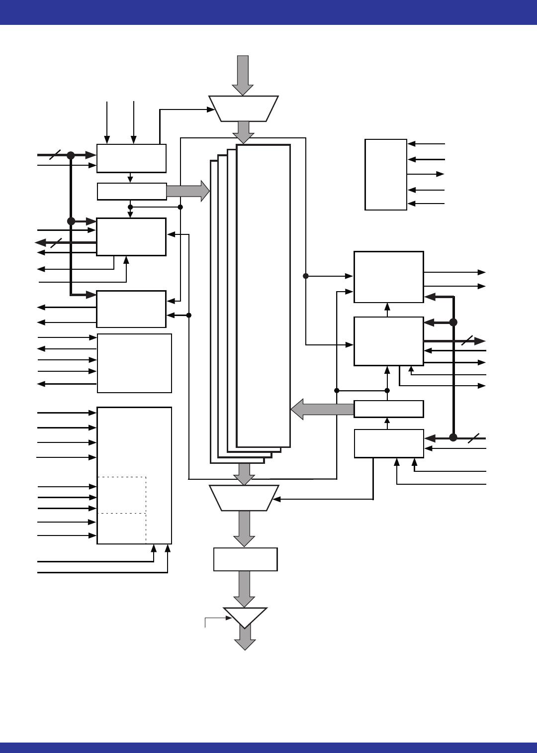
See Figure 1, Multi-Queue Flow-Control Device Block Diagram for an outline
of the functional blocks within the device.
3
IDT72V51233/72V51243/72V51253 3.3V, MULTI-QUEUE FLOW-CONTROL DEVICES
(4 QUEUES) 18 BIT WIDE CONFIGURATION 589,824, 1,179,648 and 2,359,296 bits
COMMERCIAL AND INDUSTRIAL
TEMPERATURE RANGES
OE
x9, x18
Q
out
OUTPUT
REGISTER
Q
0
- Q
17
WRADD
WADEN
INPUT
DEMUX
WCLK
WEN
Write Control
Logic
D
in
Write Pointers
Active Q
Flags
PAF
General Flag
Monitor
FSTR
PAFn
FF
FSYNC
PAF
Reset
Logic
Serial
Multi-Queue
Programming
PAE/ PAF
Offset
TMS
TDI
TDO
TCK
TRST
FM
IW
OW
PRS
MRS
SI
SO
SCLK
SENI
RCLK
REN
Read Control
Logic
Read Pointers
Active Q
Flags
PAE
General Flag
Monitor
ESTR
OV
ESYNC
RDADD
RADEN
DF
FXO
FXI
EXI
EXO
5941 drw02
x9, x18
5
6
4
ID0
ID1
ID2
Device ID
3 Bit
JTAG
Logic
SENO
DFM
MAST
PAE
Upto 4
FIFO
Queues
0.5 Mbit
1.1 Mbit
2.3 Mbit
Dual Port
Memory
OUTPUT
MUX
D
0
- D
17
PAEn
4
Figure 1. Multi-Queue Flow-Control Device Block Diagram

72V51253L6BB8

Mfr. #:
Manufacturer:
IDT
Description:
FIFO X18 4Q 2M MULTI-QUE
Lifecycle:
New from this manufacturer.
Delivery:
DHL FedEx Ups TNT EMS
Payment:
T/T Paypal Visa MoneyGram Western Union