14
COMMERCIAL AND INDUSTRIAL
TEMPERATURE RANGES
IDT72V51233/72V51243/72V51253 3.3V, MULTI-QUEUE FLOW-CONTROL DEVICES
(4 QUEUES) 18 BIT WIDE CONFIGURATION 589,824, 1,179,648 and 2,359,296 bits
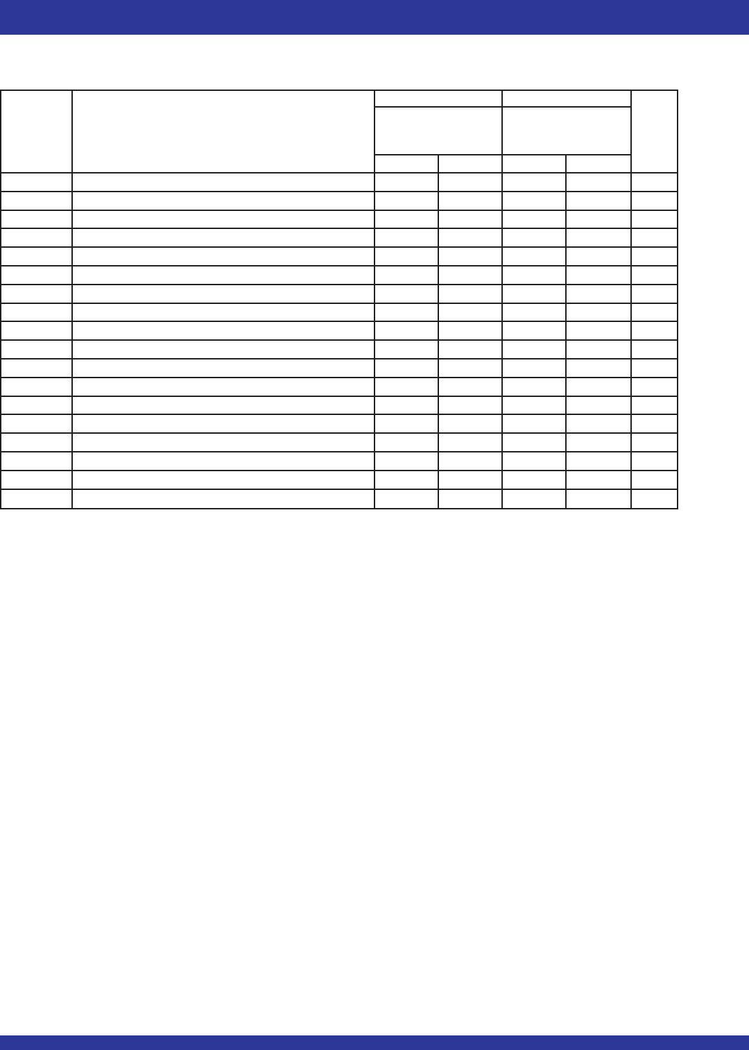
AC ELECTRICAL CHARACTERISTICS
(Commercial: VCC = 3.3V ± 0.15V, TA = 0°C to +70°C;Industrial: VCC = 3.3V ± 0.15V, TA = 40°C to +85°C; JEDEC JESD8-A compliant)
Commercial Com'l & Ind'l
(1)
IDT72V51233L6 IDT72V51233L7-5
IDT72V51243L6 IDT72V51243L7-5
IDT72V51553L6 IDT72V51553L7-5
Symbol Parameter Min. Max. Min. Max. Unit
fS Clock Cycle Frequency (WCLK & RCLK) — 166 — 133 MHz
tA Data Access Time 0.6 3.7 0.6 4 ns
tCLK Clock Cycle Time 6 — 7.5 — ns
tCLKH Clock High Time 2.7 — 3.5 — ns
tCLKL Clock Low Time 2.7 — 3.5 — ns
tDS Data Setup Time 2 — 2.0 — ns
tDH Data Hold Time 0.5 — 0.5 — ns
tENS Enable Setup Time 2 — 2.0 — ns
tENH Enable Hold Time 0.5 — 0.5 — ns
tRS Reset Pulse Width 10 — 10 — ns
tRSS Reset Setup Time 15 — 15 — ns
tRSR Reset Recovery Time 10 — 10 — ns
tPRSS Partial Reset Setup 2.0 — 2.5 — ns
tPRSH Partial Reset Hold 0.5 — 0.5 — ns
tOLZ (OE-Qn)
(2)
Output Enable to Output in Low-Impedance 0.6 3.7 0.6 4 ns
tOHZ
(2)
Output Enable to Output in High-Impedance 0.6 3.7 0.6 4 ns
tOE Output Enable to Data Output Valid 0.6 3.7 0.6 4 ns
fC Clock Cycle Frequency (SCLK) — 10 — 10 MHz
tSCLK Serial Clock Cycle 100 — 100 — ns
tSCKH Serial Clock High 45 — 45 — ns
tSCKL Serial Clock Low 45 — 45 — ns
tSDS Serial Data In Setup 20 — 20 — ns
tSDH Serial Data In Hold 1.2 — 1.2 — ns
tSENS Serial Enable Setup 20 — 20 — ns
tSENH Serial Enable Hold 1.2 — 1.2 — ns
tSDO SCLK to Serial Data Out — 20 — 20 ns
tSENO SCLK to Serial Enable Out — 20 — 20 ns
tSDOP Serial Data Out Propagation Delay 1.5 3.7 1.5 4 ns
tSENOP Serial Enable Propagation Delay 1.5 3.7 1.5 4 ns
tPCWQ Programming Complete to Write Queue Selection 20 — 20 — ns
tPCRQ Programming Complete to Read Queue Selection 20 ⎯ 20 ⎯ ns
tAS Address Setup 2.5 — 3.0 — ns
tAH Address Hold 1 — 1 — ns
tWFF Write Clock to Full Flag — 3.7 — 5 ns
tROV Read Clock to Output Valid — 3.7 — 5 ns
tSTS Strobe Setup 2 — 2 — ns
tSTH Strobe Hold 0.5 — 0.5 — ns
tQS Queue Setup 2 — 2.5 — ns
tQH Queue Hold 0.5 — 0.5 — ns
tWAF WCLK to PAF flag 0.6 3.7 0.6 4 ns
tRAE RCLK to PAE flag 0.6 3.7 0.6 4 ns
tPAF Write Clock to Synchronous Almost-Full Flag Bus 0.6 3.7 0.6 4 ns
tPAE Read Clock to Synchronous Almost-Empty Flag Bus 0.6 3.7 0.6 4 ns
NOTES:
1. Industrial temperature range product for the 7-5ns is available as a standard device. All other speed grades available by special order.
2. Values guaranteed by design, not currently tested.