3
IDT72V205/72V215/72V225/72V235/72V245 3.3V CMOS SyncFIFO
TM
256 x 18, 512 x 18, 1,024 x 18, 2,048 x 18 and 4,096 x 18
COMMERCIAL AND INDUSTRIAL
TEMPERATURE RANGES
MARCH 2013
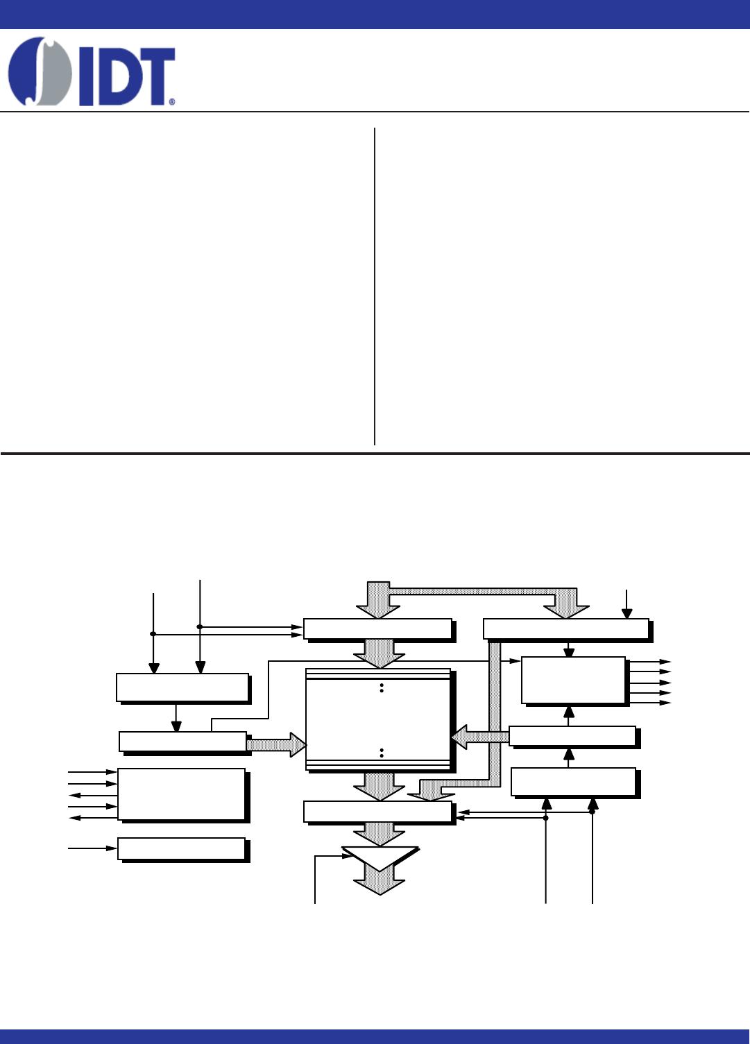
PIN DESCRIPTION
Symbol Name I/O Description
D0–D17 Data Inputs I Data inputs for an 18-bit bus.
RS Reset I When RS is set LOW, internal read and write pointers are set to the first location of the RAM array, FF and PAF
go HIGH, and PAE and EF go LOW. A reset is required before an initial WRITE after power-up.
WCLK Write Clock I When WEN is LOW, data is written into the FIFO on a LOW-to-HIGH transition of WCLK, if the FIFO is not full.
WEN Write Enable I When WEN is LOW, data is written into the FIFO on every LOW-to-HIGH transition of WCLK. When WEN is
HIGH, the FIFO holds the previous data. Data will not be written into the FIFO if the FF is LOW.
RCLK Read Clock I When REN is LOW, data is read from the FIFO on a LOW-to-HIGH transition of RCLK, if the FIFO is not empty.
REN Read Enable I When REN is LOW, data is read from the FIFO on every LOW-to-HIGH transition of RCLK. When REN is HIGH,
the output register holds the previous data. Data will not be read from the FIFO if the EF is LOW.
OE Output Enable I When OE is LOW, the data output bus is active. If OE is HIGH, the output data bus will be in a high-impedance
state.
LD Load I When LD is LOW, data on the inputs D0–D11 is written to the offset and depth registers on the LOW-to-HIGH
transition of the WCLK, when WEN is LOW. When LD is LOW, data on the outputs Q0–Q11 is read from the
offset and depth registers on the LOW-to-HIGH transition of the RCLK, when REN is LOW.
FL First Load I In the single device or width expansion configuration, FL together with WXI and RXI determine if the mode is
IDT Standard mode or First Word Fall Through (FWFT) mode, as well as whether the PAE/PAF flags are
synchronous or asynchronous. (See Table 1.) In the Daisy Chain Depth Expansion configuration, FL is
grounded on the first device (first load device) and set to HIGH for all other devices in the Daisy Chain.
WXI Write Expansion I In the single device or width expansion configuration, WXI together with FL and RXI determine if the mode
Input is IDT Standard mode or FWFT mode, as well as whether the PAE/PAF flags are synchronous or asynchronous.
(See Table 1.) In the Daisy Chain Depth Expansion configuration, WXI is connected to WXO (Write Expansion
Out) of the previous device.
RXI Read Expansion I In the single device or width expansion configuration, RXI together with FL and WXI, determine if the mode
Input is IDT Standard mode or FWFT mode, as well as whether the PAE/PAF flags are synchronous or asynchronous.
(See Table 1.) In the Daisy Chain Depth Expansion configuration, RXI is connected to RXO (Read Expansion
Out) of the previous device.
FF/IR Full Flag/ O In the IDT Standard mode, the FF function is selected. FF indicates whether or not the FIFO memory is full. In
Input Ready the FWFT mode, the IR function is selected. IR indicates whether or not there is space available for writing to
the FIFO memory.
EF/OR Empty Flag/ O In the IDT Standard mode, the EF function is selected. EF indicates whether or not the FIFO memory is empty.
Output Ready In FWFT mode, the OR function is selected. OR indicates whether or not there is valid data available at the outputs.
PAE Programmable O When PAE is LOW, the FIFO is almost-empty based on the offset programmed into the FIFO. The default
Almost-Empty Flag offset at reset is 31 from empty for IDT72V205, 63 from empty for IDT72V215, and 127 from empty for IDT72V225/
72V235/72V245.
PAF Programmable O When PAF is LOW, the FIFO is almost-full based on the offset programmed into the FIFO. The default offset at
Almost-Full Flag reset is 31 from full for IDT72V205, 63 from full for IDT72V215, and 127 from full for IDT72V225/72V235/72V245.
WXO/HF Write Expansion O In the single device or width expansion configuration, the device is more than half full when HF is LOW. In the
Out/Half-Full Flag depth expansion configuration, a pulse is sent from WXO to WXI of the next device when the last location in the
FIFO is written.
RXO Read Expansion O In the depth expansion configuration, a pulse is sent from RXO to RXI of the next device when the last
Out location in the FIFO is read.
Q0–Q17 Data Outputs O Data outputs for an 18-bit bus.
VCC Power +3.3V power supply pins.
GND Ground Seven ground pins.