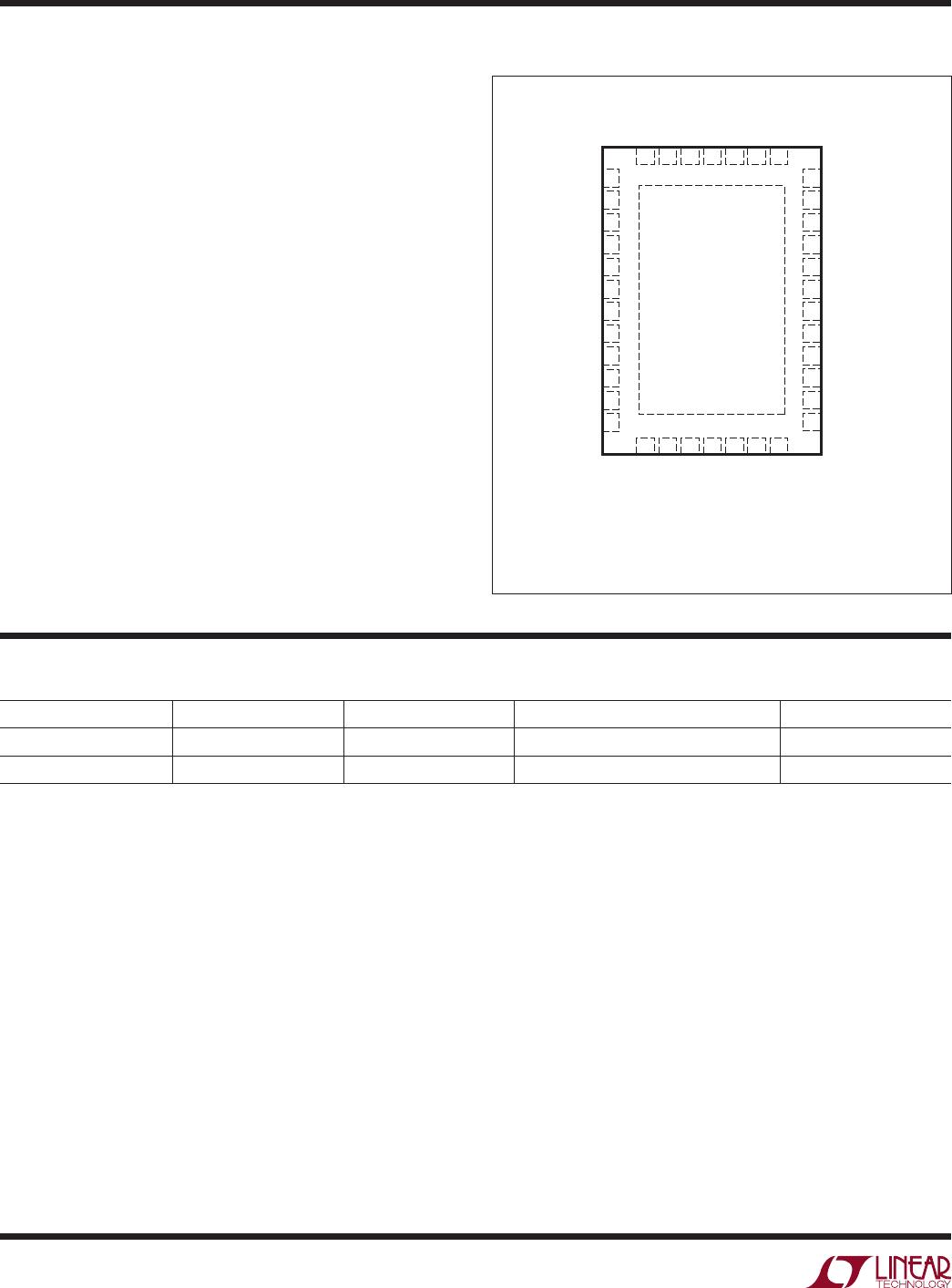
LTC2872
1
2872f
Typical applicaTions
DescripTion
RS232/RS485 Dual
Multiprotocol Transceiver
with Integrated Termination
The LTC
®
2872 is a robust pin-configurable transceiver
that supports RS232, RS485, and RS422 standards while
operating on a single 3V to 5.5V supply. The LTC2872 can
be configured as four RS232 single-ended transceivers
or two RS485 differential transceivers, or combinations
of both, on shared I/O lines.
Pin-controlled integrated termination resistors allow
for easy interface reconfiguration, eliminating external
resistors and control relays. Half-duplex switches allow
four-wire and two-wire RS485 configurations. Loopback
mode steers the driver inputs to the receiver outputs for
diagnostic self-test. The RS485 receivers support up to
256 nodes per bus, and feature full failsafe operation for
floating, shorted or terminated inputs.
An integrated DC/DC boost converter uses a small induc-
tor and one capacitor, eliminating the need for multiple
supplies for driving RS232 levels.
L, LT, LTC, LTM, Linear Technology, the Linear logo and µModule are registered trademarks of
Linear Technology Corporation. All other trademarks are the property of their respective owners.
RS485 Mode with Duplex Control
FeaTures
applicaTions
n
Four RS232 and Two RS485 Transceivers
n
3V to 5.5V Supply Voltage
n
20Mbps RS485 and 500kbps RS232
n
Automatic Selection of Integrated RS485 (120Ω)
and RS232 (5kΩ) Termination Resistors
n
Half-/Full-Duplex RS485 Switching
n
Logic Loopback Mode
n
High ESD: ±16kV on Line I/O
n
1.7V to 5.5V Logic Interface
n
Supports Up to 256 RS485 Nodes
n
RS485 Receiver Full Failsafe Eliminates UART Lockup
n
Available in 38-Pin 5mm × 7mm QFN Package
n
Flexible RS232/RS485/RS422 Interface
n
Software Selectable Multiprotocol Interface Ports
n
Point-of-Sale Terminals
n
Cable Repeaters
n
Protocol Translators
n
PROFIBUS-DP Networks
RS232 Mode Mixed Mode with RS485 Termination
2872 TA01
LTC2872
3V TO 5.5V1.7V TO V
CC
RS485
TERMINATION
H/F
DY1
2.2µF
Y1
Z1
A2
B2
A1
B1
RA1
DY2
RA2
V
DD
V
EE
DY1
DY2
RB2
RA2
DZ2
RB1
RA1
DZ1
Y1
B2
A2
Z1
Y2
Z2
A1
B1
LTC2872
DY2
RB2
RA2
DZ2
B2
A2
Y2
Z2
Y1
Z1
DY1
TE485-1
LTC2872
120Ω
ONOFF
RS485
DUPLEX
HALFFULL
Y2
Z2
A1
B1
RA1
120Ω
V
L
V
CC
CAP
470nF
22µH
2.2µF
2.2µF
2.2µF
2.2µF
2.2µF
2.2µF2.2µF 2.2µF 2.2µF
SW
3V TO 5.5V1.7V TO V
CC
2.2µF
V
DD
V
EE
V
L
V
CC
CAP
470nF
22µH
SW
3V TO 5.5V1.7V TO V
CC
2.2µF
V
DD
V
EE
V
L
V
CC
CAP
470nF
22µH
SW
LTC2872
2
2872f
pin conFiguraTionabsoluTe MaxiMuM raTings
Input Supplies
V
CC
, V
L
..................................................... 0.3V to 7V
Generated Supplies
V
DD
................................................ V
CC
– 0.3V to 7.5V
V
EE
.........................................................0.3V to –7.5V
V
DD
– V
EE
..............................................................15V
SW ........................................... 0.3V to (V
DD
+ 0.3V)
CAP ............................................. 0.3V to (V
EE
– 0.3V)
A1, A2, B1, B2, Y1, Y2, Z1, Z2 ......................15V to 15V
DY1, DY2, DZ1, DZ2, RXEN1, RXEN2, DXEN1, DXEN2,
LB, H/F, TE485_1, TE485_2,
485/232 _1, 485/232_2 ................................ 0.3V to 7V
FEN, RA1, RA2, RB1, RB2 ...............0.3V to (V
L
+ 0.3V)
Differential Enabled Terminator Voltage
(A1-B1 or A2-B2 or Y1-Z1 or Y2-Z2) .....................±6V
Operating Temperature
LTC2872C ................................................ 0°C to 70°C
LTC2872I .............................................40°C to 85°C
Storage Temperature Range .................. 65°C to 125°C
(Note 1)
13 14 15 16
TOP VIEW
39
V
EE
UHF PACKAGE
38-LEAD (5mm × 7mm) PLASTIC QFN
17 18 19
38 37 36 35 34 33 32
24
25
26
27
28
29
30
31
8
7
6
5
4
3
2
1V
CC
A1
B1
Y1
GND
Z1
DY1
DZ1
RXEN1
DXEN1
TE485_1
TE485_2
V
CC
A2
B2
Y2
GND
Z2
DY2
DZ2
RXEN2
DXEN2
V
CC
V
DD
RB1
RA1
LB
V
L
GND
RA2
RB2
485/232_1
485/232_2
H/F
FEN
CAP
GND
SW
23
22
21
20
9
10
11
12
T
JMAX
= 125°C, θ
JA
= 34.7°C/W
EXPOSED PAD (PIN #39) IS V
EE
, MUST BE SOLDERED TO PCB
orDer inForMaTion
LEAD FREE FINISH TAPE AND REEL PART MARKING* PACKAGE DESCRIPTION TEMPERATURE RANGE
LTC2872CUHF#PBF LTC2872CUHF#TRPBF 2872
38-Lead (5mm × 7mm) Plastic QFN
0°C to 70°C
LTC2872IUHF#PBF LTC2872IUHF#TRPBF 2872
38-Lead (5mm × 7mm) Plastic QFN
–40°C to 85°C
Consult LTC Marketing for parts specified with wider operating temperature ranges. *The temperature grade is identified by a label on the shipping container.
Consult LTC Marketing for information on non-standard lead based finish parts.
For more information on lead free part marking, go to: http://www.linear.com/leadfree/
For more information on tape and reel specifications, go to: http://www.linear.com/tapeandreel/
LTC2872
3
2872f
elecTrical characTerisTics
The l denotes the specifications which apply over the full operating
temperature range, otherwise specifications are at T
A
= 25°C. V
CC
= V
L
= 3.3V, TE485_1 = TE485_2 = 0V, LB = 0V unless otherwise noted.
SYMBOL PARAMETER CONDITIONS MIN TYP MAX UNITS
Power Supply
V
CC
Supply Voltage Operating Range
l
3 5.5 V
V
L
Logic Supply Voltage Operating Range V
L
≤ V
CC
l
1.7 V
CC
V
V
CC
Supply Current in Shutdown Mode RXEN1 = RXEN2 = V
L
,
DXEN1 = DXEN2 = FEN = H/F = 0V
l
8 60 µA
V
CC
Supply Current in RS485 Transceiver Mode
(Outputs Unloaded) (Note 3)
485/232_1 = 485/232_2 = DXEN1 =
DXEN2 = V
L
, RXEN1 = RXEN2 = 0V
l
4.5 7 mA
V
CC
Supply Current in RS232 Transceiver Mode
(Outputs Unloaded) (Note 3)
DXEN1 = DXEN2 = V
L
; 485/232_1 =
485/232_2 = RXEN1 = RXEN2 = 0V
l
5.5 8 mA
V
L
Supply Current in RS485 or RS232 Transceive
Mode (Outputs Unloaded)
DXEN1 = DXEN2 = V
L
, RXEN1 = RXEN2 = 0V
l
0 5 µA
RS485 Drivers
|V
OD
| Differential Output Voltage R
L
= ∞, V
CC
= 3V (Figure 1)
R
L
= 27Ω, V
CC
= 4.5V (Figure 1)
R
L
= 27Ω, V
CC
= 3V (Figure 1)
R
L
= 50Ω, V
CC
= 3.13V (Figure 1)
l
l
l
l
2.1
1.5
2
6
V
CC
V
CC
V
CC
V
V
V
V
∆|V
OD
| Difference in Magnitude of Differential Output
Voltage for Complementary Output States
R
L
= 27Ω, V
CC
= 3V (Figure 1)
R
L
= 50Ω, V
CC
= 3.13V (Figure 1)
l
l
0.2
0.2
V
V
V
OC
Common Mode Output Voltage R
L
= 27Ω or 50Ω (Figure 1)
l
3 V
∆|V
OC
| Difference in Magnitude of Common Mode
Output Voltage for Complementary Output States
R
L
= 27Ω or 50Ω (Figure 1)
l
0.2 V
I
OZD485
Three-State (High Impedance) Output Current V
OUT
= 12V or –7V,
V
CC
= 0V or 3.3V (Figure 2)
l
–100 125 µA
I
OSD485
Maximum Short-Circuit Current –7V ≤ V
OUT
≤ 12V (Figure 2)
l
–250 250 mA
RS485 Receiver
I
IN485
Input Current V
IN
= 12V or –7V, V
CC
= 0V or 3.3V
(Figure 3) (Note 5)
l
–100 125 µA
R
IN485
Input Resistance V
IN
= 12V or –7V, V
CC
= 0V or 3.3V
(Figure 3) (Note 5)
125
Differential Input Signal Threshold Voltage (A–B) –7V ≤ (A or B) ≤ 12 (Note 5)
l
±200 mV
Differential Input Signal Hysteresis B = 0V (Notes 3, 5) 190 mV
Differential Input DC Failsafe Threshold Voltage
(A–B)
–7V ≤ (A or B) ≤ 12 (Note 5)
l
–200 –65 0 mV
Differential Input DC Failsafe Hysteresis B = 0V (Note 5) 30 mV
V
OL
Output Low Voltage Output Low, I(RA) = 3mA (Sinking),
3V ≤ V
L
≤ 5.5V
l
0.4 V
Output Low, I(RA) = 1mA (Sinking),
1.7V ≤ V
L
< 3V
l
0.4 V
V
OH
Output High Voltage Output High, I(RA) = –3mA (Sourcing),
3V ≤ V
L
≤ 5.5V
l
V
L
– 0.4 V
Output High, I(RA) = –1mA (Sourcing),
1.7V ≤ V
L
< 3V
l
V
L
– 0.4 V
Three-State (High Impedance) Output Current 0V ≤ RA ≤ V
L
, V
L
= 5.5V
l
0 ±5 μA
Short-Circuit Output Current 0V ≤ RA ≤ V
L
, V
L
= 5.5V
l
±135 mA
R
TERM
Terminating Resistor TE485 = V
L
, A–B = 2V, B = –7V, 0V, 10V
(Figure 8) (Note 5)
l
108 120 156 Ω

LTC2872IUHF#PBF

Mfr. #:
Manufacturer:
Analog Devices Inc.
Description:
RS-232 Interface IC RS232/RS485 Dual Port Multiprotocol Transceiver with Integrated Termination (Shared I/O)
Lifecycle:
New from this manufacturer.
Delivery:
DHL FedEx Ups TNT EMS
Payment:
T/T Paypal Visa MoneyGram Western Union