LTC2872
16
2872f
FuncTion Tables
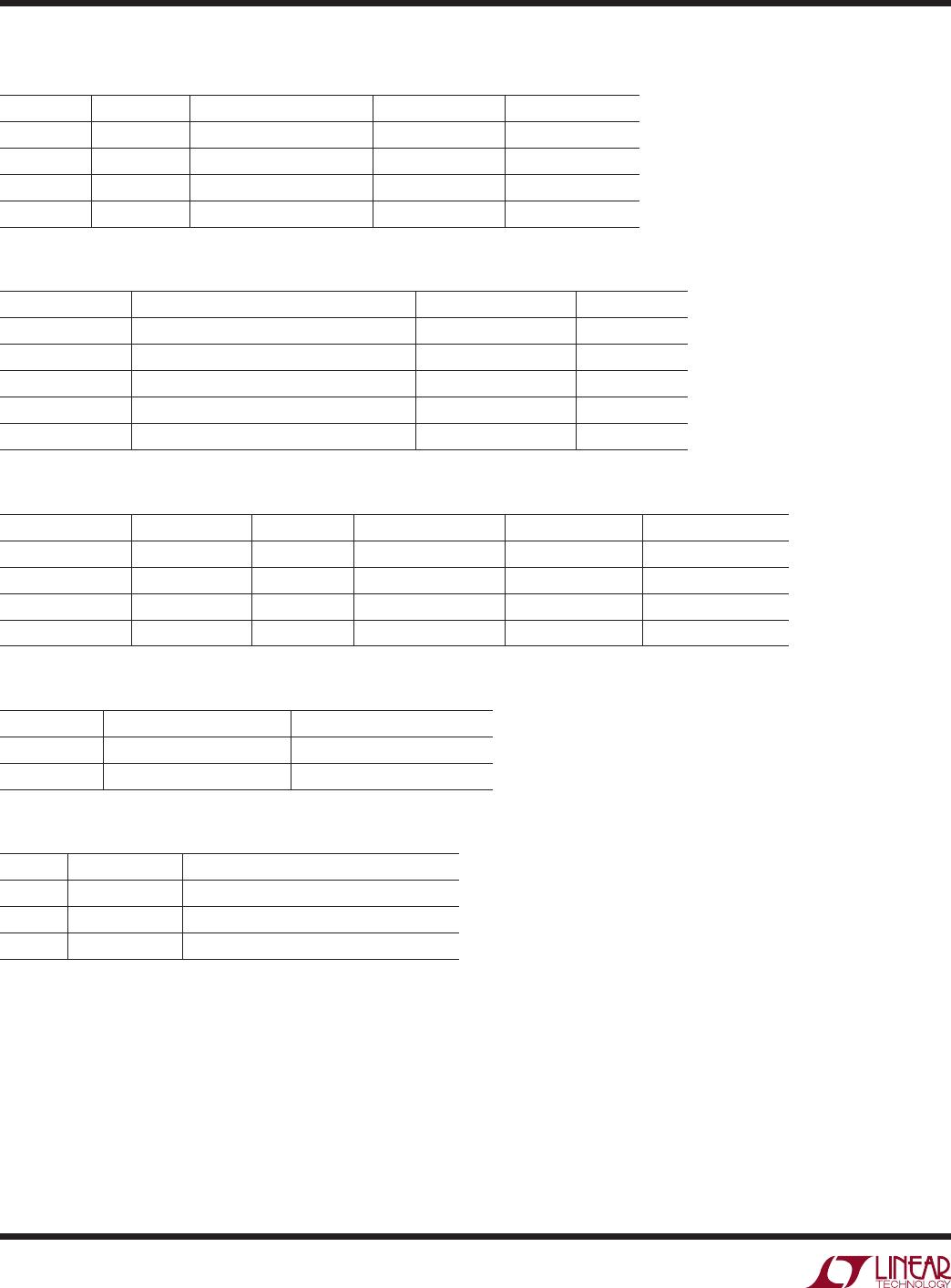
Table 5. RS485 Driver Mode for a Given Port (485/232 = 1, TE485 = 0)
DXEN DY CONDITIONS Y Z
0 X No Fault 125kΩ 125kΩ
1 0 No Fault 0 1
1 1 No Fault 1 0
X X Thermal Fault 125kΩ 125kΩ
Table 6. RS485 Receiver Mode for a Given Port (485/232 = 1, LB = 0)
RXEN A–B (NOTE 5) CONDITIONS RA
1 X No Fault Hi-Z
0 < –200mV No Fault 0
0 > 200mV No Fault 1
0 Inputs Open or Shorted Together (DC) No Fault 1
X X Thermal Fault Hi-Z
Table 7. RS485 Termination for a Given Port (485/232 = 1)
TE485 DZ H/F, LB CONDITIONS R(A TO B) R(Y TO Z)
0 X X No Fault Hi-Z Hi-Z
1 0 X No Fault 120Ω Hi-Z
1 1 X No Fault 120Ω 120Ω
X X X Thermal Fault Hi-Z Hi-Z
Table 8. RS485 Duplex Control for Given Port (485/232 = 1)
H/F RS485 DRIVER OUTPUTS RS485 RECEIVER INPUTS
0 Y, Z A, B
1 Y, Z Y, Z
Table 9. Loopback Functions for a Given Port
LB RXEN TRANSCEIVER MODE
0 X Not Loopback
1 1 Not Loopback
1 0 Loopback (RA = DY, RB = DZ)
LTC2872
17
2872f
Overview
The LTC2872 is a flexible multiprotocol transceiver sup-
porting RS485/RS422 and RS232 protocols. It can be
powered from a single 3.0V to 5.5V supply with optional
logic interface supply as low as 1.7V. An integrated DC/
DC converter provides the positive and negative supply
rails needed for RS232 operation. Automatically selected
integrated termination resistors for both RS232 and
RS485 protocols are included, eliminating the need for
external components and switching relays. Both parts
include loopback control for self-test and debug as well
as logically-switchable half- and full-duplex control of the
RS485 bus interface.
The LTC2872 offers two ports that can be independently
configured as either two RS232 receivers and drivers or
one RS485/RS422 receiver and driver depending on the
state of its 485/232 pins. Control inputs DXEN and RXEN
provide independent control of driver and receiver opera-
tion for either RS232 or RS485 transceivers, depending
on the selected operating protocol.
The LTC2872 features rugged operation with an ESD rating
of ±15kV HBM on the receiver inputs and driver outputs,
both powered and unpowered. All other pins offer protec-
tion exceeding ±4kV.
DC/DC Converter
The on-chip DC/DC converter operates from the V
CC
input,
generating a 7V V
DD
supply and a charge pumped –6.3V
V
EE
supply, as shown in Figure 13. V
DD
and V
EE
power
the output stage of the RS232 drivers and are regulated
to levels that guarantee greater than ±5V output swing.
The DC/DC converter requires a 22µH inductor (L1) and a
bypass capacitor (C4) of 2.2µF or larger. The charge pump
capacitor (C1) is 470nF and the storage capacitors (C2 and
C3) are 2.2µF. Larger storage capacitors up to 4.7µF may
be used if C1 and C4 are scaled proportionately. Locate
C1-C4 close to their associated pins.
Bypass capacitor C5 on the logic supply pin can be omitted
if V
L
is connected to V
CC
. See the V
L
Logic Supply section
for more details about the V
L
logic supply.
Inductor Selection
An inductor with a value of 22µH ±20% is required. It
must have a saturation current (I
SAT
) rating of at least
200mA and a DCR (copper wire resistance) of less than
1.3Ω. Some small inductors meeting these requirements
are listed in Table 10.
Table 10. Recommended Inductors
PART NUMBER
L
(µH)
I
SAT
(mA)
MAX
DCR
(Ω) SIZE (mm) MANUFACTURER
BRC2016T220M
CBC2518T220M
22
22
310
320
1.3
1.0
2 × 1.6 × 1.6
2.5 × 1.8 × 1.8
Taiyo Yuden
t-yuden.com
LQH32CN220K53 22 250 0.92 3.2 × 2.5 × 1.6 Murata
murata.com
Capacitor Selection
The small size of ceramic capacitors makes them ideal for
the LTC2872. Use X5R or X7R dielectric types; their ESR is
low and they retain their capacitance over relatively wide
voltage and temperature ranges. Use a voltage rating of
at least 10V.
applicaTions inForMaTion
Figure 13. DC/DC Converter with Required External Components
2872 F13
BOOST
REGULATOR
V
CC
3V TO 5.5V
V
L
1.7V TO V
CC
C1
470nF
L1
22µH
21
18
C4
2.2µF
V
CC
V
DD
V
EE
SW
GND
GND
CAP
C5
0.1µF
C2
2.2µF
19
C3
2.2µF
17
20
39
34
V
L
35
LTC2872
18
2872f
Inrush Current and Supply Overshoot Precaution
In certain applications fast supply slew rates are gener-
ated when power is connected. If V
CC
s voltage is greater
than 4.5V and its rise time is faster than 10μs, the pins
V
DD
and SW can exceed their Absolute Maximum values
during start-up. When supply voltage is applied to V
CC
, the
voltage difference between V
CC
and V
DD
generates inrush
current flowing through inductor L1 and capacitors C1 and
C2. The peak inrush current must not exceed 2A. To avoid
this condition, add a 1Ω resistor as shown in Figure 14.
This precaution is not relevant for supply voltages below
4.5V or rise times longer than 10μs.
by more than 1V for proper operation. Logic input pins
do not have internal biasing devices to pull them up or
down. They must be driven high or low to establish valid
logic levels; do not float.
RS485 Driver
The RS485 driver provides full RS485/RS422 compat-
ibility. When enabled, if DI is high, Y–Z is positive. When
the driver is disabled, Y and Z output resistance is greater
than 96k (typically 125k) to ground over the entire common
mode range of –7V to 12V. This resistance is equivalent
to the input resistance on these lines when the driver is
configured in half-duplex mode and Y and Z act as the
RS485 receiver inputs.
Driver Overvoltage and Overcurrent Protection
The RS232 and RS485 driver outputs are protected from
short circuits to any voltage within the Absolute Maximum
range ±15V. The maximum current in this condition is
90mA for the RS232 driver and 250mA for the RS485 driver.
If an RS485 driver output is shorted to a voltage greater
than V
CC
, when active high, positive current of about
100mA can flow from the driver output back to V
CC
. If the
system power supply or loading cannot sink this excess
current, clamp V
CC
to GND with a Zener diode (e.g., 5.6V,
1W, 1N4734) to prevent an overvoltage condition on V
CC
.
All devices also feature thermal shutdown protection that
disables the drivers, receivers, and RS485 terminators in
case of excessive power dissipation (see Note 6).
RS485 Balanced Receiver with Full Failsafe Support
The LTC2872 RS485 receiver has a differential threshold
voltage that is about 80mV for signals that are rising
and –80mV for signals that are falling, as illustrated in
Figure 15. If a differential input signal lingers in the win-
dow between these thresholds for more than about 2µs,
the rising threshold changes from 80mV to –50mV, while
the falling threshold remains at –80mV. Thus, differential
inputs that are shorted, open, or terminated but not driven
for more than 2µs produce a high on the receiver output,
indicating a failsafe condition.
applicaTions inForMaTion
Figure 14. Supply Current Overshoot Protection
for Input Supplies of 4.5V of Higher
V
L
Logic Supply
A separate logic supply pin V
L
allows the LTC2872 to
interface with any logic signal from 1.7V to 5.5V. All logic
I/Os use V
L
as their high supply. For proper operation, V
L
should not be greater than V
CC
. During power-up, if V
L
is higher than V
CC
, the device will not be damaged, but
behavior of the device is not guaranteed. If V
L
is not con-
nected to V
CC
, bypass V
L
with a 0.1µF capacitor.
RS232 and RS485 driver outputs are undriven and the
RS485 termination resistors are disabled when V
L
or V
CC
is grounded or V
CC
is disconnected.
Although all logic input pins reference V
L
as their high
supply, they can be driven up to 7V, independent of V
L
and
V
CC
, with the exception of FEN, which must not exceed V
L
2872 F14
0V
5V
≤10µs
C1
470nF
L1
22µH
INRUSH
CURRENT
C4
2.2µF
R1
1/8W
V
CC
V
DD
GND
SW
19 17
CAP
20
21
18
C2
2.2µF
LTC2872IUHF#PBF

Mfr. #:
Manufacturer:
Analog Devices Inc.
Description:
RS-232 Interface IC RS232/RS485 Dual Port Multiprotocol Transceiver with Integrated Termination (Shared I/O)
Lifecycle:
New from this manufacturer.
Delivery:
DHL FedEx Ups TNT EMS
Payment:
T/T Paypal Visa MoneyGram Western Union