LTC2872
7
2872f
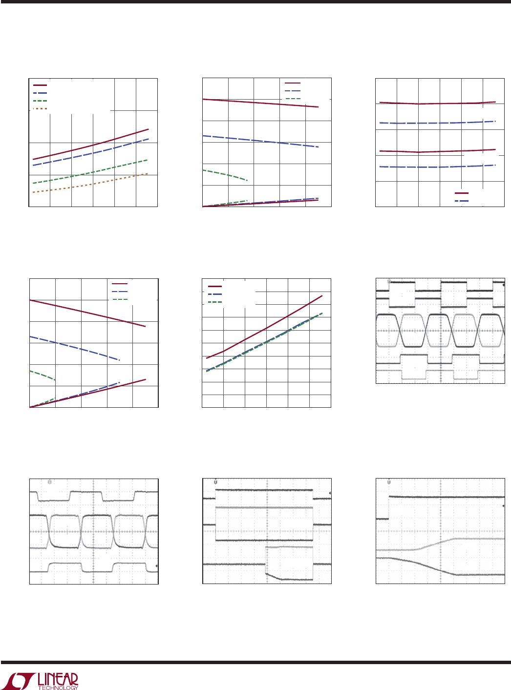
Typical perForMance characTerisTics
RS485 Termination Resistance
vs Temperature RS232 Operation at 500kbps
RS485 Operation at 20Mbps
RS485 Receiver Output Voltage
vs Load Current
RS232 Receiver Input Threshold
vs Temperature
RS232 Receiver Output Voltage
vs Load Current
RS232 Driver Outputs Enabling
and Disabling V
DD
and V
EE
Powering Up
RS485 Receiver Propagation
Delay vs Temperature
TEMPERATURE (°C)
–50
DELAY (ns)
80
70
60
50
40
50 75–25
2872 G10
100250
V
CC
= 3.3V, V
L
= 1.7V
V
CC
= 5V, V
L
= 1.7V
V
CC
= 3.3V, V
L
= 3.3V
V
CC
= 5V, V
L
= 5V
OUTPUT CURRENT (mA)
0
OUTPUT VOLTAGE (V)
6
5
4
2
3
1
0
82
2872 G11
1064
V
L
= 5V
V
L
= 3.3V
V
L
= 1.7V
TEMPERATURE (°C)
–50
THRESHOLD VOLTAGE (V)
2.0
1.8
1.6
1.4
1.2
1.0
50 75–25
2872 G12
100250
V
CC
= 5V
V
CC
= 3.3V
INPUT HIGH
INPUT LOW
OUTPUT CURRENT (mA)
0
OUTPUT VOLTAGE (V)
6
5
4
2
3
1
0
82
2872 G13
1064
V
L
= 5V
V
L
= 3.3V
V
L
= 1.7V
TEMPERATURE (°C)
–50
RESISTANCE (Ω)
130
118
116
114
112
110
128
126
124
122
120
50 75–25
2872 G14
100250
V
CM
= –7V
V
CM
= 2V
V
CM
= 12V
1µs/DIV
WRAPPING DATA
DOUT LOADS: 5kΩ + 50pF
5V/DIV
2872 G15
DY
DZ
RA
RB
Z
Y
20ns/DIV
H/F HIGH
Y, Z LOADS: 120Ω (DIFF) + 50pF
1V/DIV
5V/DIV
5V/DIV
2872 G16
DY
RA
Z
Y
40ns/DIV
5V/DIV
2872 G17
DXEN
FEN = VL
FEN = 0V
Z
Y
Z
Y
100µs/DIV
5V/DIV
2V/DIV
2872 G18
FEN
V
DD
V
EE
LTC2872
8
2872f
pin FuncTions
V
CC
(Pins 1, 21, 31): Input Supply (3.0V to 5.5V). Tie all
three pins together and connect 2.2µF capacitor between
VCC and GND.
V
L
(Pin 35): Logic Supply (1.7V to 5.5V) for the receiver
outputs, driver inputs, and control inputs. This pin should
be bypassed to GND with a 0.1µF capacitor if it is not tied
to V
CC
. V
L
must be less than or equal to V
CC
for proper
operation.
V
DD
(Pin 20): Generated Positive Supply Voltage for RS232
Driver (7V). Connect 2.2µF capacitor between V
DD
and GND.
V
EE
(Pin 39):Generated Negative Supply Voltage for RS232
Driver (–6.3V). Tie all pins together and connect 2.2µF
capacitor between V
EE
and GND.
GND (Pins 5, 18, 27, 34): Ground. Tie all four pins together.
CAP (Pin 17): Charge Pump Capacitor for Generated Nega-
tive Supply Voltage. Connect a 470nF capacitor between
CAP and SW.
SW (Pin 19): Switch Pin. Connect 22µH inductor between
SW and V
CC
.
A1 (Pin 2): RS485 Differential Receiver #1 Positive Input
(Full-Duplex Mode) or RS232 Receiver #1a Input.
A2 (Pin 30): RS485 Differential Receiver #2 Positive Input
(Full-Duplex Mode) or RS232 Receiver #2a Input.
B1 (PIn 3): RS485 Differential Receiver #1 Negative Input
(Full-Duplex Mode) or RS232 Receiver #1b Input.
B2 (Pin 29): RS485 Differential Receiver #1 Negative Input
(Full-Duplex Mode) or RS232 Receiver #2b Input.
RA1 (Pin 37): RS485 Differential Receiver #1 Output or
RS232 Receiver #1a Output.
RA2 (Pin 33): RS485 Differential Receiver #2 Output or
RS232 Receiver #2a Output.
RB1 (Pin 38): RS232 Receiver #1b Output.
RB2 (Pin 32): RS232 Receiver #2b Output.
DY1 (Pin 7): RS485 Differential Driver #1 Input or RS232
Driver #1y Input.
DY2 (Pin 25): RS485 Differential Driver #2 Input or RS232
Driver #2y Input.
DZ1 (Pin 8): RS232 Driver #1z Input.
DZ2 (Pin 24): RS232 Driver #2z Input.
Y1 (Pin 4): RS485 Differential Driver #1 Positive Output
or RS232 Driver #1y Output, RS485 Differential Receiver
#1 Positive Input (Half-Duplex Mode).
Y2 (Pin 28): RS485 Differential Driver #2 Positive Output
or RS232 Driver #2y Output, RS485 Differential Receiver
#2 Positive Input (Half-Duplex Mode).
Z1 (Pin 6): RS485 Differential Driver #1 Negative Output
or RS232 Driver #1z Output, RS485 Differential Receiver
#1 Negative Input (Half-Duplex Mode).
Z2 (Pin 26): RS485 Differential Driver #2 Negative Output
or RS232 Driver #2z Output, RS485 Differential Receiver
#2 Negative Input (Half-Duplex Mode).
485/232_1 (Pin 13): Interface Select #1 Input. A logic low
enables RS232 mode and a high enables RS485 mode for
transceiver #1. The mode determines which transceiver
inputs and outputs are accessible at the LTC2872 pins
as well as which is controlled by the driver and receiver
enable pins.
485/232_2 (Pin 14): Interface Select #2 Input. A logic low
enables RS232 mode and a high enables RS485 mode for
transceiver #2. The mode determines which transceiver
inputs and outputs are accessible at the LTC2872 pins
as well as which is controlled by the driver and receiver
enable pins.
RXEN1 (Pin 9): Receivers #1 Enable. A logic high disables
RS232 and RS485 receivers in transceiver #1, leaving their
outputs Hi-Z. A logic low enables the RS232 or RS485
receivers in transceiver #1, depending on the state of the
Interface Select Input 485/232_1.
RXEN2 (Pin 23): Receivers #2 Enable. A logic high disables
RS232 and RS485 receivers in transceiver #2, leaving their
outputs Hi-Z. A logic low enables the RS232 or RS485
receivers in transceiver #2, depending on the state of the
Interface Select Input 485/232_2.
LTC2872
9
2872f
pin FuncTions
DXEN1 (Pin 10): Drivers #1 Enable. A logic low disables the
RS232 and RS485 drivers in transceiver #1, leaving their
outputs in a Hi-Z state. A logic high enables the RS232 or
RS485 drivers in transceiver #1, depending on the state
of the Interface Select Input 485/232_1.
DXEN2 (Pin 22): Drivers #2 Enable. A logic low disables the
RS232 and RS485 drivers in transceiver #2, leaving their
outputs in a Hi-Z state. A logic high enables the RS232 or
RS485 drivers in transceiver #2, depending on the state
of the Interface Select Input 485/232_2.
TE485_1 (Pin 11): RS485 Termination Enable for Trans-
ceiver #1. A logic high enables a 120Ω resistor between
pins A1 and B1. If DZ1 is also high, a 120Ω resistor is
enabled between pins Y1 and Z1. A logic low on TE485_1
opens the resistors, leaving A1/B1 and Y1/Z1 unterminated,
independent of DZ1. The differential termination resistors
are never enabled in RS232 mode.
TE485_2 (Pin 12): RS485 Termination Enable for Trans-
ceiver #2. A logic high enables a 120Ω resistor between
pins A2 and B2. If DZ2 is also high, a 120Ω resistor is
enabled between pins Y2 and Z2. A logic low on TE485_2
opens the resistors, leaving A2/B2 and Y2/Z2 unterminated,
independent of DZ2. The differential termination resistors
are never enabled in RS232 mode.
H/F (Pin 15): RS485 Half-duplex Select Input for Trans-
ceivers #1 and #2. A logic low is used for full duplex
operation where pins A and B are the receiver inputs and
pins Y and Z are the driver outputs. A logic high is used
for half duplex operation where pins Y and Z are both the
receiver inputs and driver outputs and pins A and B do
not serve as the receiver inputs. The impedance on A and
B and state of differential termination between A and B is
independent of the state of H/F. The H/F pin has no effect
on RS232 operation.
FEN (Pin 16): Fast Enable. A logic high enables Fast Enable
Mode. In fast enable mode the integrated DC/DC converter
is active independent of the state of driver, receiver, and
termination enable pins allowing faster circuit enable
times than are otherwise possible. A logic low disables
Fast Enable Mode leaving the state of the DC/DC converter
dependent on the state of driver, receiver, and termina-
tion enable control inputs. The DC/DC converter powers
down only when FEN is low and all drivers, receivers, and
terminators are disabled (refer to Table 1).
LB (Pin 36): Loopback Enable for Transceivers #1 and #2.
A logic high enables Logic Loopback diagnostic mode,
internally routing the driver input logic levels to the receiver
output pins within the same transceiver. This applies to
both RS232 channels as well as the RS485 driver/receiver.
The targeted receiver must be enabled for the loopback
signal to be available on its output. A logic low disables
loopback mode. In loopback mode, signals are not inverted
from driver inputs to receiver outputs.

LTC2872IUHF#PBF

Mfr. #:
Manufacturer:
Analog Devices Inc.
Description:
RS-232 Interface IC RS232/RS485 Dual Port Multiprotocol Transceiver with Integrated Termination (Shared I/O)
Lifecycle:
New from this manufacturer.
Delivery:
DHL FedEx Ups TNT EMS
Payment:
T/T Paypal Visa MoneyGram Western Union