LTC2872
19
2872f
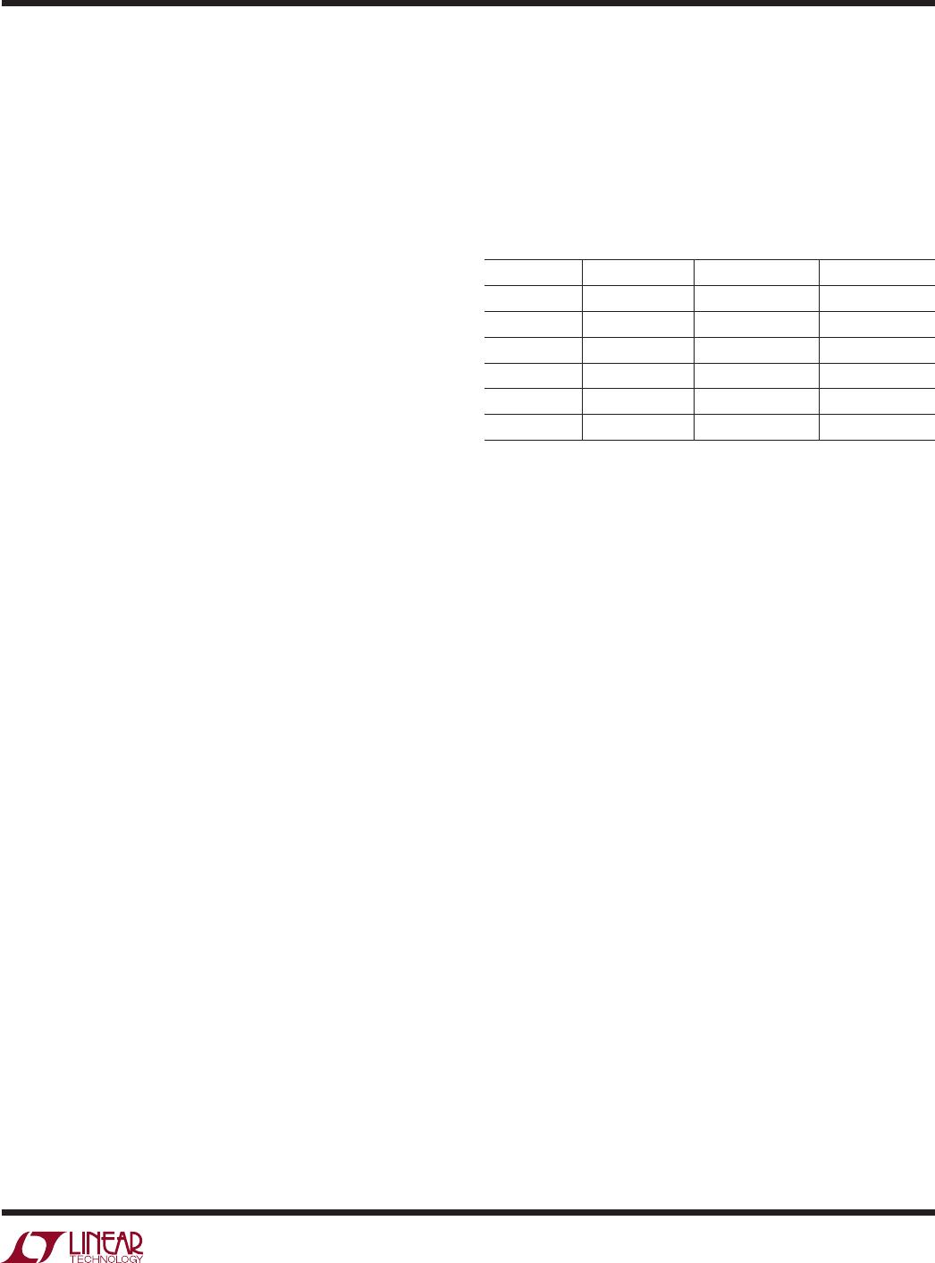
Figure 15. RS485 Receiver Input Threshold
Characteristics with Typical Values Shown
applicaTions inForMaTion
The benefit of this dual threshold architecture is that
it supports full failsafe operation yet offers a balanced
threshold, centered on 0V, for normal data signals. This
balance preserves duty cycle for small input signals with
heavily slewed edges, typical of what might be seen at the
end of a very long cable. This performance is highlighted
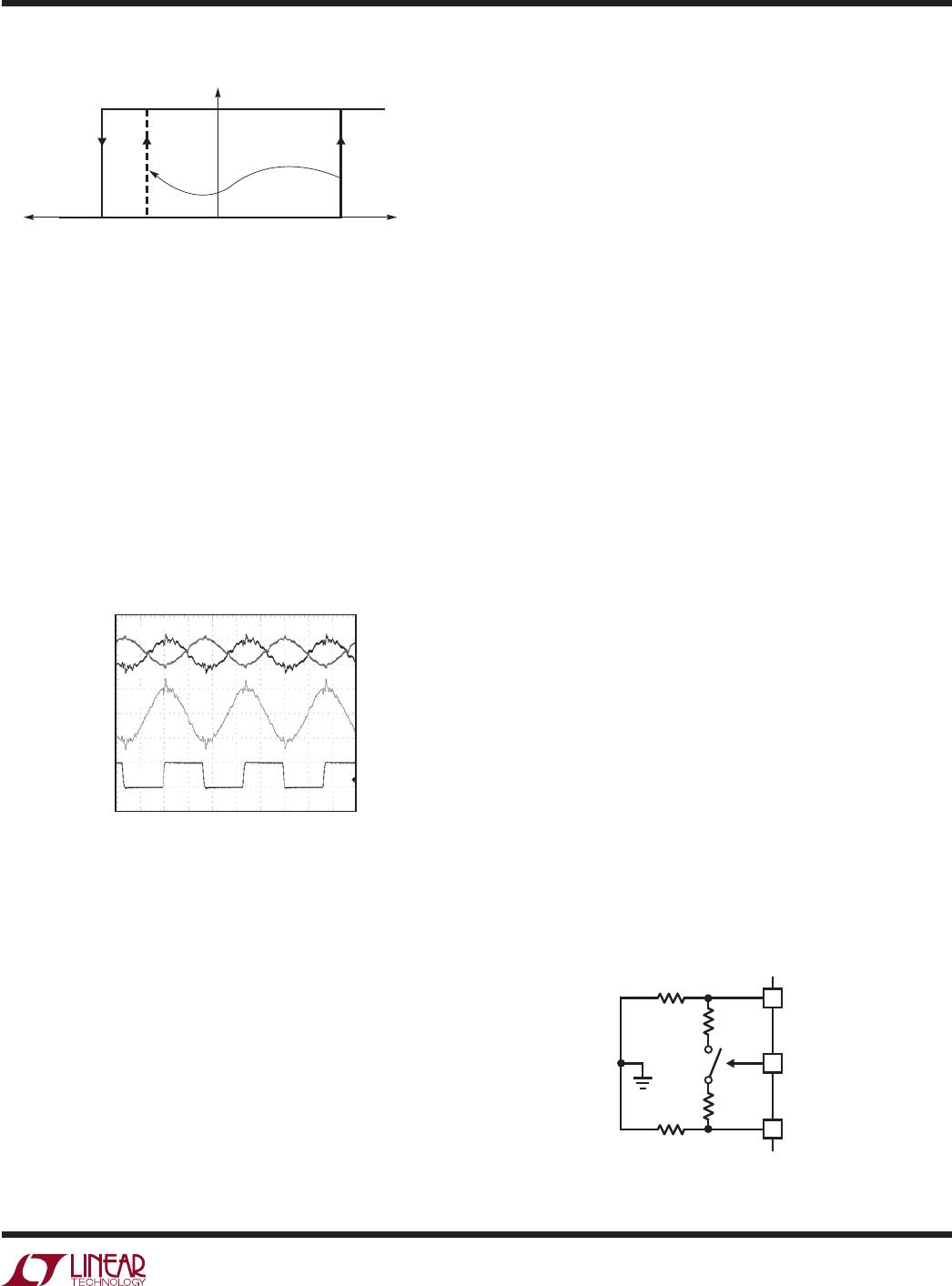
in Figure 16, where a signal is driven through 4000 feet
of CAT5e cable at 3Mbps. Even though the differential
signal peaks at just over 100mV and is heavily slewed,
the output maintains a nearly perfect signal with almost
no duty cycle distortion.
lines, which establishes a logic-high state when all the
transmitters on the network are disabled. The values of
the biasing resistors depend on the number and type
of transceivers on the line and the number and value of
terminating resistors. Therefore, the values of the biasing
resistors must be customized to each specific network
installation, and may change if nodes are added to or
removed from the network.
The internal failsafe feature of the LTC2872 eliminates the
need for external network biasing resistors provided they
are used in a network of transceivers with similar internal
failsafe features. This also allows the network to support a
high number of nodes, up to 256, by eliminating the bias
resistor loading. The LTC2872 transceivers will operate
correctly on biased, unbiased, or under-biased networks.
Receiver Outputs
The RS232 and RS485 receiver outputs are internally
driven high (to V
L
) or low (to GND) with no external pull-up
needed. When the receivers are disabled, the output pin
becomes Hi-Z with leakage of less than ±5μA for voltages
within the V
L
supply range.
RS485 Receiver Input Resistance
The RS485 receiver input resistance from A or B to GND
(Y or Z to GND in half-duplex mode with driver disabled)
is greater than 96k (typically 125k) when the integrated
termination is disabled. This permits up to a total of 256
receivers per system without exceeding the RS485 receiver
loading specification. The input resistance of the receiver
is unaffected by enabling/disabling the receiver or whether
the part is in half-duplex, full-duplex, loopback mode, or
even unpowered. The equivalent input resistance looking
into the RS485 receiver pins is shown in Figure 17.
Figure 16. A 3Mbps Signal Driven Down 4000ft of CAT5e
Cable. Top Traces: Received Signals After Transmission
Through Cable; Middle Trace: Math Showing Differences
of Top Two Signals; Bottom Trace: Receiver Output
An additional benefit of the balanced architecture is excel-
lent noise immunity due to the wide effective differential
input signal hysteresis of 160mV for signals transitioning
through the window region in less than 2μs. Increasingly
slower signals will have increasingly less effective hyster-
esis, limited by the DC failsafe hysteresis of about 30mV.
RS485 Biasing Network Not Required
RS485 networks are often biased with a resistive divider
to generate a differential voltage of ≥200mV on the data
0.1V/DIV
0.1V/DIV
5V/DIV
2872 F16
200ns/DIV
RA
(A-B)
A
B
Figure 17. Equivalent RS485 Receiver
Input Resistance Into A and B (Note 5)
2872 F17
A
B
TE485
60Ω
60Ω
125k
125k
2872 F15
–80mV –50mV 0V
RA
80mV
V
AB
(NOTE 5)
RISING THRESHOLD
SHIFTS IF SIGNAL IS
IN WINDOW > ~2µs
TO SUPPORT
FAILSAFE
LTC2872
20
2872f
applicaTions inForMaTion
Selectable RS485 Termination
Proper cable termination is important for good signal fidel-
ity. When the cable is not terminated with its characteristic
impedance, reflections cause waveform distortion.
The LTC2872 offers integrated switchable 120Ω termination
resistors between the differential receiver inputs and also
between the differential driver outputs. This provides the
advantage of being able to easily change, through logic
control, the proper line termination for correct operation
when configuring transceiver networks. Termination should
be enabled on transceivers positioned at both ends of a
network bus.
Termination on the driver nodes is important for cases
where the driver is disabled but there is communication on
the connecting bus from another node. Driver termination
across Y and Z can be disabled independently from the
termination across A and B by setting DZ low. See Table 7
for details.
The termination resistance is maintained over the entire
RS485 common mode range of –7V to 12V as shown in
Figure 18. The voltage across pins with the terminating
resistor enabled should not exceed 6V as indicated in the
Absolute Maximum Ratings table.
Figure 18. Typical Resistance of the Enabled RS485
Terminator vs Common Mode Voltage of A and B
the differential receiver inputs. With the H/F pin set to
a logic-high, the Y and Z pins serve as the differential
inputs. In either configuration, the RS485 driver outputs
are always on Y and Z. The impedance looking into the
A and B pins is not affected by H/F control, including the
differential termination resistance. The H/F control does
not affect RS232 operation.
Logic Loopback
A loopback mode connects the driver inputs to the re-
ceiver outputs (noninverting) for self test. This applies
to both RS232 and RS485 transceivers. Loopback mode
is entered when the LB pin is set to a logic-high and the
relevant receiver is enabled.
In loopback mode, the drivers function normally. They
can be disabled with output in a Hi-Z state or left enabled
to allow loopback testing in normal operation. Loopback
works in half- or full-duplex modes and does not affect
the termination resistors.
RS485 Cable Length vs Data Rate
Many factors contribute to the maximum cable length
that can be used for for RS485 or RS422 communication,
including driver transition times, receiver threshold, duty
cycle distortion, cable properties and data rate. A typical
curve of cable length versus maximum data rate is shown
in Figure 19. Various regions of this curve reflect different
performance limiting factors in data transmission.
Figure 19. Cable Length vs Data Rate (RS485/RS422
Standard Shown in Vertical Solid Line)
RS485 Half- and Full-Duplex Control
The LTC2872 is equipped with a control to change the RS485
transceiver operation from full-duplex to half-duplex. With
the H/F pin set to a logic-low, the A and B pins serve as
DATA RATE (bps)
CABLE LENGTH (FT)
2872 F19
10k
1k
100
10
10k 10M 100M1M100k
LTC2872
MAX DATA RATE
RS485/RS422
MAX DATA RATE
VOLTAGE (V)
–10
RESISTANCE (Ω)
126
124
122
118
120
116
10–5
2872 F18
1550
V
CC
= 5.0V
V
CC
= 3.3V
LTC2872
21
2872f
applicaTions inForMaTion
At frequencies below 100kbps, the maximum cable length
is determined by DC resistance in the cable. In this ex-
ample, a cable longer than 4000ft will attenuate the signal
at the far end to less than what can be reliably detected
by the receiver.
For data rates above 100kbps, the capacitive and inductive
properties of the cable begin to dominate this relation-
ship. The attenuation of the cable is frequency and length
dependent, resulting in increased rise and fall times at
the far end of the cable. At high data rates or long cable
lengths, these transition times become a significant part
of the signal bit time. Jitter and intersymbol interference
aggravate this so that the time window for capturing valid
data at the receiver becomes impossibly small.
The boundary at 20Mbps in Figure 19 represents the
guaranteed maximum operating rate of the LTC2872. The
dashed vertical line at 10Mbps represents the specified
maximum data rate in the RS485 standard. This boundary
is not a limit, but reflects the maximum data rate that the
specification was written for.
It should be emphasized that the plot in Figure 19 shows
a typical relation between maximum data rate and cable
length. Results with the LTC2872 will vary, depending on
cable properties such as conductor gauge, characteristic
impedance, insulation material, and solid versus stranded
conductors.
Layout Considerations
All V
CC
pins must be connected together and all ground
pins must be connected together on the PC board with
very low impedance traces or dedicated planes. A 2.2µF,
or larger, bypass capacitor should be placed less than
0.7cm away from V
CC
Pin 21. This V
CC
pin, as well as GND
Pin 18, mainly service the DC/DC converter. Additional
bypass capacitors of 0.1µF or larger, can be added to V
CC
Pins 1 and 31 if the traces back to the 2.2µF capacitor
are indirect or narrow. These V
CC
pins mainly service the
transceivers #1 and #2, respectively. Table 11 summarizes
the bypass capacitor requirements. The capacitors listed
in the table should be placed closest to their respective
supply and ground pin.
Table 11. Bypass Capacitor Requirements
CAPACITOR SUPPLY (PIN) RETURN (PIN) COMMENT
2.2µF V
CC
(21) GND (18) Required
2.2 µF V
DD
(20) GND (18) Required
2.2uF V
EE
(39) GND (18) Required
0.1µF V
L
(35) GND (34) Required*
0.1µF V
CC
(1) GND (5) Optional
0.1µF V
CC
(31) GND (27) Optional
* If V
L
is not connected to V
CC
.
Place the charge pump capacitor, C1, directly adjacent to
the SW and CAP pins, with no more than one centimeter
of total trace length to maintain low inductance. Close
placement of the inductor, L1, is of secondary importance
compared to the placement of C1 but should include no
more than two centimeters of total trace length.
The PC board traces connected to high speed signals A/B
and Y/Z should be symmetrical and as short as possible
to minimize capacitive imbalance and to maintain good
differential signal integrity. To minimize capacitive loading
effects, the differential signals should be separated by
more than the width of a trace and should not be routed
on top of each other if they are on different signal planes.
Care should be taken to route outputs away from any sen-
sitive inputs to reduce feedback effects that might cause
noise, jitter, or even oscillations. For example, DI and A/B
should not be routed near the driver or receiver outputs.

LTC2872IUHF#PBF

Mfr. #:
Manufacturer:
Analog Devices Inc.
Description:
RS-232 Interface IC RS232/RS485 Dual Port Multiprotocol Transceiver with Integrated Termination (Shared I/O)
Lifecycle:
New from this manufacturer.
Delivery:
DHL FedEx Ups TNT EMS
Payment:
T/T Paypal Visa MoneyGram Western Union