IDT
®
Low Power Clock for Intel Atom
®
-Based Systems 1561C — 08/24/11
9LPRS436C
Low Power Clock for Intel Atom
®
-Based Systems
10
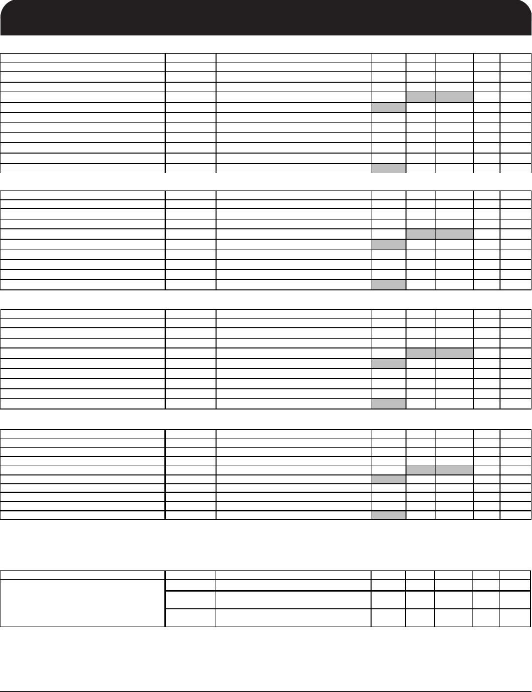
Electrical Characteristics - USB48MHz, 12/48MHz
PARAMETER SYMBOL CONDITIONS MIN
TY P
MAX UNITS
NOTES
Lon
Accurac
m see T
eriod min-max values -100 100
m1,2
Clock pe riod T
period
48.00MHz output nominal 20.83125 20.83542 ns 2,3
Absolute min/max period
T
abs
48.00MHz output nominal 20.48125 21.18542 ns 2
Output High Voltage V
OH
I
OH
= -1 mA 2.4 V 1
Output Low Voltage V
OL
I
OL
= 1 mA 0.4 V 1
Rising Edge Slew Rate (USB48M)
t
SLR
Measured from 0.8 to 2.0 V 1 1.7 2 V/ns 1
Falling Edge Slew Rate (USB48M) t
FLR
Measured from 2.0 to 0.8 V 1 1.7 2 V/ns 1
Rising Edge Slew Rate (12/48M)
t
SLR
Measured from 0.8 to 2.0 V 1 1.7 2 V/ns 1
Fallin g Edge Slew Rate (12/48M) t
FLR
Measured from 2.0 to 0.8 V 1 1.7 2 V/ns 1
Duty Cycle
d
t1
V
T
= 1.5 V 45 50.6 55 % 1
Jitter, Cycle to cycle
t
jcyc-cyc
V
T
= 1.5 V 150 350 ps
1
Electrical Characteristics - 25MHz
PARAMETER SYMBOL CONDITIONS MIN
TY P
MAX UNITS
NOTES
Lon
Accurac
m see T
eriod min-max values -100 0 100
m1,2
Clock pe riod T
period
25.00MHz output nominal 39.99600 40.00400 ns 2,3
Absolute min/max period
T
abs
25.00MHz output nominal 39.32360 40.67640 ns 2
Output High Voltage V
OH
I
OH
= -1 mA 2.4 V 1
Output Low Voltage V
OL
I
OL
= 1 mA 0.4 V 1
Rising Edge Slew Rate
t
SLR
Measured from 0.8 to 2.0 V 1 1.8 2 V/ns 1
Falling Edge Slew Rate t
FLR
Measured from 2.0 to 0.8 V 1 1.8 2 V/ns 1
Duty Cycle
d
t1
V
T
= 1.5 V 45 49.6 55
%1
Jitter, Cycle to cycle t
jcyc-cyc
V
T
= 1.5 V 150 500 ps 1
Electrical Characteristics - 12.288MHz
PARAMETER SYMBOL CONDITIONS MIN
TY P
MAX UNITS
NOTES
Lon
Accurac
m see T
eriod min-max values -100 0 100
m1,2
Clock pe riod T
period
12.288MHz output nominal 81.37207 81.38835 ns 2,3
Absolute min/max period
T
abs
12.288MHz output nominal 80.87207 81.88835 ns 2
Output High Voltage V
OH
I
OH
= -1 mA 2.4 V 1
Output Low Voltage V
OL
I
OL
= 1 mA 0.4 V 1
Rising Edge Slew Rate
t
SLR
Measured from 0.8 to 2.0 V 1 1.8 2 V/ns 1
Falling Edge Slew Rate t
FLR
Measured from 2.0 to 0.8 V 1 1.8 2 V/ns 1
Duty Cycle
d
t1
V
T
= 1.5 V 45 50.1 55
%1
Jitter, Cycle to cycle t
jcyc-cyc
V
T
= 1.5 V 133 500 ps 1
Electrical Characteristics - REF-14.318MHz
PARAMETER SYMBOL CONDITIONS MIN TYP MAX UNITS Notes
Long Accuracy ppm see Tperiod min-max values -100 0 100 ppm 1,2
Clock pe riod Tperiod 14.318MHz output nominal 69.82033 69.86224 ns 2,3
Absolute min/max period Tabs 14.3 18MHz output nominal 69.83400 70.84800 ns 2
Output High Voltage VOH IOH = -1 mA 2.4 V 1
Output Low Voltage VOL IOL = 1 mA 0.4 V 1
Rising Edge Slew Rate tSLR Measure d from 0.8 to 2.0 V 1 1.5 4 V/ns 1
Fallin
Ed
e Slew Rate tFL R Measure d from 2.0 to 0.8 V 1 1.4 4 V/ns 1
Dut
C
cle dt1 VT = 1.5 V 45 50.2 55 % 1
Jitter, C
cle to c
cle t
c
c-c
VT = 1.5 V 139 1000
s1
*T
A
= Tambient ; V
DD
= 3.3 V +/-5%; C
L
=5pF, Rs=22
Ω
(unless specified otherwise)
1
Guaranteed by design and characterization, not 100% tested in p rod uction.
2
All Long Term Accuracy and Clock Period specifications are guaranteed assuming that REFOUT is at 14.31818MHz
3
The average period over any 1us period of time
Electrical Characteristics - Phase Jitter
PARAMETER SYMBOL CONDITIONS MIN TYP. MAX UNITS
NOTES
t
jp hPCIe1
PCIe Gen 1 REFCLK phase jitter 30 86 ps 1 ,2,3
t
jph PCIe2Lo
PCIe Gen 2 REFCLK phase jitter
Lo-band content
1.3 3
ps
RMS
1,2,3
t
jphPC Ie2Hi
PCIe Gen 2 REFCLK phase jitter
Hi-band content
1.7 3.1
ps
RMS
1,2,3
*T
A
= Tambient; V
DD
= 3.3 V +/-5%; C
L
=5pF , Rs=22
Ω
(unless specified otherwise)
Notes on Phase Ji tter:
2
Device driven b
932S421BGLF or e
uivalent
2
Sam
le size of at least 100K c
cles. This fi
ures extra
olates to 108
s
k-
k @ 1M c
cles for a BER of 1
-12
3
A
lies to PCIEX
3:0
out
uts onl
.
1
See htt
:/ /www.
cisi
.com f or c om
lete s
ecs. Guaranteed b
desi
n and characterization, not tested in
roduction.
Jitter, Phase