IDT
®
Low Power Clock for Intel Atom
®
-Based Systems 1561C — 08/24/11
9LPRS436C
Low Power Clock for Intel Atom
®
-Based Systems
13
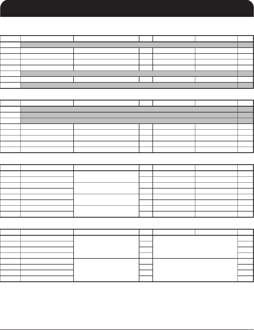
SMBus Table: Frequency Select Register
Byte 0 Name Control Function Type 0 1 PWD
Bit 7
Reserved 0
Bit 6
Reserved 0
Bit 5
Spread Enable
Enables Spread for
CPU/SRC/PCI outputs
RW Off 0.5% down spread 0
Bit 4
FS4 Freq Select Bit 4 RW Latch
Bit 3
FS3 Freq Select Bit 3 RW Latch
Bit 2
FSLC Freq Select Bit 2 RW Latch
Bit 1
FSLB Freq Select Bit 1 RW Latch
Bit 0
FSLA Freq Select Bit 0 RW Latch
SMBus Table: Output Control Register
Byte 1 Name Control Function Type 0 1 PWD
Bit 7
DOT96Mhz Output Enable RW Disable Enable 1
Bit 6
SATA/PCIe3 Output Enable RW Disable Enable 1
Bit 5
ITP/PCIe2 Output Enable RW Disable Enable 1
Bit 4
PCIe1 Output Enable RW Disable Enable 1
Bit 3
PCIe0 Output Enable RW Disable Enable 1
Bit 2
12.288MHz
Output Enable (Disabling This
output also disables the
12.288M PLL).
RW Disable Enable 1
Bit 1
25MHz
25MHz free running during VDD
Suspend (S-states). If this bit is
set to 0, the XTAL OSC will also
be powered down in the
Suspend States)
RW Does Not Run Runs 1
Bit 0
CPU PLL MN_EN CPU PLL M/N Enable RW Disable Enable 0
SMBus Table: Output Control Register
Byte 2 Name Control Function Type 0 1 PWD
Bit 7
USB_48MHz Output Enable RW Disable Enable 1
Bit 6
0
Bit 5
REF0 Output Enable RW Disable Enable 1
Bit 4
25MHz Output Enable RW Disable Enable 1
Bit 3
12_48MHz Output Enable RW Disable Enable 1
Bit 2
PCICLK_F0 Output Enable RW Disable Enable 1
Bit 1
PCICLK0 Output Enable RW Disable Enable 1
Bit 0
0
SMBus Table: Output Control Register
Byte 3 Name Control Function Type 0 1 PWD
Bit 7
CPUCLK1 Output Enable RW Disable Enable 1
Bit 6
CPUCLK0 Output Enable RW Disable Enable 1
Bit 5
PEREQ3# Control PCIEX1 is controlled RW Not Controlled Controlled 0
Bit 4
PEREQ3# Control PCIEX2 is controlled RW Not Controlled Controlled 0
Bit 3
PEREQ2# Control PCIEX1 is controlled RW Not Controlled Controlled 0
Bit 2
PEREQ2# Control SATACLK is controlled RW Not Controlled Controlled 0
Bit 1
PEREQ1# Control PCIEX0 is controlled RW Not Controlled Controlled 0
Bit 0
PEREQ1# Control SATACLK is controlled RW Not Controlled Controlled 0
NOTE: Only 1 PEREQ at a time can be selected to control an output.
Reserved
Reserved
See Table 1: CPU/SRC/PCI PLL
Frequency Selection Table
IDT
®
Low Power Clock for Intel Atom
®
-Based Systems 1561C — 08/24/11
9LPRS436C
Low Power Clock for Intel Atom
®
-Based Systems
14
SMBus Table: Output Control and Readback Register
Byte 4 Name Control Function 0 1 PWD
Bit 7
0
Bit 6
CPU_1 Free-Running Control RW Free-Running Stoppable 0
Bit 5
SEL_12_48 SEL12_48MHz readback R 48MHz 12MHz latch
Bit 4
CPUCLK_2/ITP Free-Running Control RW Free-Running Stoppable 0
Bit 3
ITP_EN ITP_EN readback R PCIEX6 CPU_ITP latch
Bit 2
0
Bit 1
CPUCLK_0 Free-Running Control RW Free-Running Stoppable 0
Bit 0
0
SMBus Table: Output Control Register
Byte 5 Name Control Function 0 1 PWD
Bit 7
0
Bit 6
0
Bit 5
0
Bit 4
SATA/PCIe3 Free- Running Control RW Free-Running Stoppable 1
Bit 3
PCIe2 Free- Running Control RW Free-Running Stoppable 0
Bit 2
PCIe1 Free- Running Control RW Free-Running Stoppable 0
Bit 1
PCIe0 Free- Running Control RW Free-Running Stoppable 0
Bit 0
Load Control IIC Load control RW Load Do not Load 0
SMBus Table: Amplitude Control Register
Byte 6 Name Control Function Type 0 1 PWD
Bit 7
Diff AMP RW 00 = 700mV 10 = 900mV 0
Bit 6
Diff AMP RW 01 = 800mV 11 = 1000mV 1
Bit 5
Diff AMP RW 00 = 700mV 10 = 900mV 0
Bit 4
Diff AMP RW 01 = 800mV 11 = 1000mV 1
Bit 3
Diff AMP RW 00 = 700mV 10 = 900mV 0
Bit 2
Diff AMP RW 01 = 800mV 11 = 1000mV 1
Bit 1
Diff AMP RW 00 = 700mV 10 = 900mV 0
Bit 0
Diff AMP RW 01 = 800mV 11 = 1000mV 1
SMBus Table: Revision and Vendor ID Register
Byte 7 Name Control Function Type 0 1 PWD
Bit 7
RID3 R x
Bit 6
RID2 R x
Bit 5
RID1 R x
Bit 4
RID0 R x
Bit 3
VID3 R 0
Bit 2
VID2 R 0
Bit 1
VID1 R 0
Bit 0
VID0 R 1
0010 = C Rev
VENDOR ID
SATA/PCIe3 Differential output
Amplitude Control
DOT96 Differential output
Amplitude Control
Reserved
Reserved
Reserved
Revision ID
0001 = ICS
CPU Differential output
Amplitude Control
Reserved
Reserved
Reserved
PCIe(2:0) Differential output
Amplitude Control
IDT
®
Low Power Clock for Intel Atom
®
-Based Systems 1561C — 08/24/11
9LPRS436C
Low Power Clock for Intel Atom
®
-Based Systems
15
SMBus Table: Byte Count Register
Byte 8 Name Control Function Type 0 1 PWD
Bit 7
Reserved 0
Bit 6
Reserved 0
Bit 5
Reserved 0
Bit 4
BC4 RW 0
Bit 3
BC3 RW 1
Bit 2
BC2 RW 1
Bit 1
BC1 RW 1
Bit 0
BC0 RW 1
SMBus Table: Watch Dog Timer Control Register
Byte 9 Name Control Function Type 0 1 PWD
Bit 7
HWD_EN Watchdog Hard Alarm Enable RW Disable Enable 0
Bit 6
WD Hard Status WD Hard Alarm Status R Normal Alarm X
Bit 5
WDTCtrl
Watch Dog Alarm Time base
Control
R0
Bit 4
HWD3 WD Hard Alarm Timer Bit 3 RW 1
Bit 3
HWD2 WD Hard Alarm Timer Bit 2 RW 1
Bit 2
HWD1 WD Hard Alarm Timer Bit 1 RW 1
Bit 1
HWD0 WD Hard Alarm Timer Bit 0 RW 1
Bit 0
Reserved Reserved RW - - 0
SMBus Table: Skew programming Register
Byte 10 Name Control Function Type 0 1 PWD
Bit 7
CPUSkw3 RW 0
Bit 6
CPUSkw2 RW 0
Bit 5
CPUSkw1 RW 0
Bit 4
CPUSkw0 RW 0
Bit 3
CPUSkw3 RW 0
Bit 2
CPUSkw2 RW 0
Bit 1
CPUSkw1 RW 0
Bit 0
CPUSkw0 RW 0
CPU Skew Programming Table
Byte 10 bits [7:4]
or bits [3:0]
Skew Value (ps)
0000 0
0001 100
0010 200
0011 300
0100 400
0101 500
0110 600
0111 700
1000 800
1001 900
1010 1000
1011 1100
1100 1200
1101 1300
1110 1400
1111 1500
290ms Base
CPUCLK0 Skew Control (ps)
Writing to this register will configure how
many bytes will be read back, default is
0F = 15 bytes.
Byte Count Programming
These bits represent X*290ms or X*1.16s.
The watchdog timer waits before it goes to
alarm mode. Default is 15 X 290ms =
4.35s.
CPUCLK1 Skew Control (ps)
See CPU Skew Programming Table

9LPRS436CKILF

Mfr. #:
Manufacturer:
IDT
Description:
Clock Generators & Support Products ATOM NETTOP/NETBOOK
Lifecycle:
New from this manufacturer.
Delivery:
DHL FedEx Ups TNT EMS
Payment:
T/T Paypal Visa MoneyGram Western Union