IDT
®
Low Power Clock for Intel Atom
®
-Based Systems 1561C — 08/24/11
9LPRS436C
Low Power Clock for Intel Atom
®
-Based Systems
4
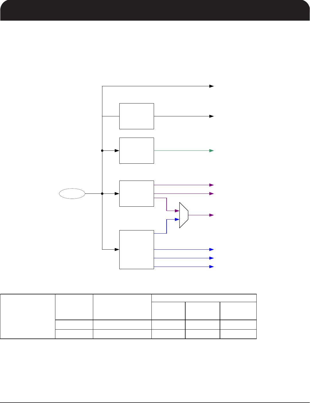
Pin Description (Continued)
25 GND PWR Ground
in.
26 VDDPCIEX PWR Power suppl
for PCI Express clocks, nominal 3.3V
27 CPUITPC_LR2/PCIeC_LR2 OUT
Complementary clock of differential pair CPU output. / Complementary clock of
differential PCIEX pair. These are 0.8V push pull outputs. No external 50ohm
resistor to GND or 33ohm series resistor needed.
28 CPUITPT_LR2/PCIeT_LR2 OUT
True clock of differential pair CPU output. / True clock of differential PCIEX
pair. These are 0.8V push pull outputs. No external 50ohm resistor to GND or
33ohm series resistor needed.
29 CPUC_LR1 OUT
Complementary clock of differential pair 0.8V push-pull CPU outputs with
inte
rated 33ohm series resistor.
30 CPUT_LR1 OUT
True clock of differential pair 0.8V push-pull CPU outputs with integrated
33ohm series resistor.
31 VDDCPU PWR Su
l
for CPU clocks, 3.3V nominal
32 CPUC_LR0 OUT
Complementary clock of differential pair 0.8V push-pull CPU outputs with
inte
rated 33ohm series resistor.
33 CPUT_LR0 OUT
True clock of differential pair 0.8V push-pull CPU outputs with integrated
33ohm series resistor.
34 GND PWR Ground pin.
35 SCLK IN Clock pin of SMBus circuitr
, 5V tolerant.
36 SDATA I/O Data
in for SMBus circuitr
, 5V tolerant.
37 CPU_STOP# IN Sto
s CPU0 clock when enabled.
38 PCI&PCIEX_STOP# IN
Stops all PCICLKs at logic 0 level, when low. Free running PCICLKs are not
effected b
this in
ut.
39 X2_25 OUT Cr
stal out
ut, Nominall
25.00MHz.
40 X1_25 IN Cr
stal input, Nominall
25.00MHz.
41 GND PWR Ground
in.
42 25MHz OUT 25MHz clock out
ut, 3.3V
43 VDDSUSP PWR
Supply for suspend mode, powers 25MHz PLL, 25M output and XTAL
oscillator. 3.3V Nominal
44 Vtt_PwrGd/WOL_STOP# IN
This active high 3.3V LVTTL input is a level sensitive strobe used to determine
when latch inputs are valid and are ready to be sampled / Asynchronous active
low input pin that stops all outputs except free running 25Mhz
45 VDD14 PWR Power for 14.31818MHz PLL and REF out
ut, nominal 3.3V.
46 REF0_2x/FSLC I/O
2x strength 14.318 MHz reference clock./ 3.3V tolerant input for CPU frequency
selection. Refer to input electrical characteristics for Vil_FS and Vih_FS
values.
47 GND PWR Ground pin.
48 GND PWR Ground
in.