IDT
®
Low Power Clock for Intel Atom
®
-Based Systems 1561C — 08/24/11
9LPRS436C
Low Power Clock for Intel Atom
®
-Based Systems
9
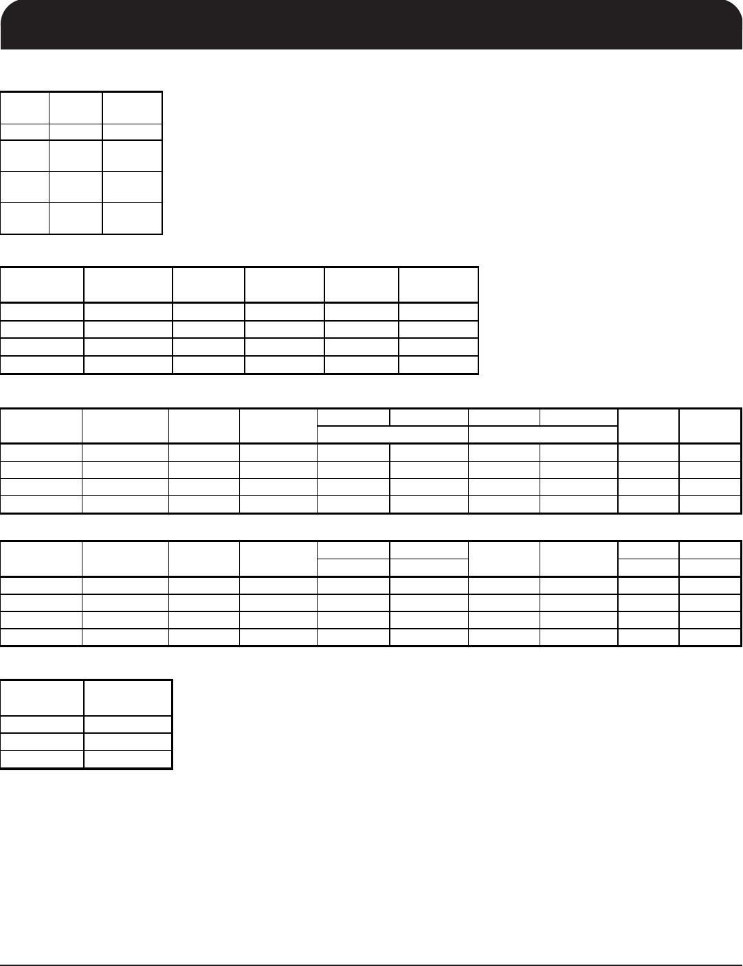
AC Electrical Characteristics - Input/Common Parameters
PARAMETER SYMBOL CONDITIONS MIN TYP MAX UNITS Notes
C lk Stabilization
T
STAB
From VDD Power-Up or de-assertion of PD to
1st clock
1.1 1 .8 ms
Td rive_PEREQ_off
T
DRPEROFF
Output stop after PEREQ# deasserted 2 3 clocks
Td rive_PEREQ_on T
DRPERON
Output run after PEREQ# a sserted 2 3 clocks
Tdrive_CPU
T
DRSR C
CPU output enable after
CPU_STOP# de-assertion
810ns
Tdrive_PCIEX
T
DRPCIEX
PCIEX output enab le after
PCI&PCIEX_STOP# de-assertion
815ns1
Tfall_SE
T
FALL
10 ns
Trise_SE T
RISE
10 ns
Td r iv e_P D#
T
DRPD
Differential output enable after
PD# de-assertion
85 300 us 1
Fall/rise time of all 3.3V control inputs from 20-
80%
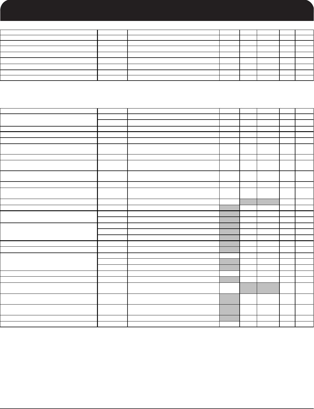
AC Electrical Characteristics - CPU, PCIEX, SATA, DOT96MHz
P ARAME TE R SYMB O L C OND ITIONS M IN TY P MA X UNITS NOTE S
Rising Edge Slew Rate tSLR Different ial Measurement 2.5 3.3 4 V/ns 1,2
Falling Edge Slew Rate tFLR Differential Measurement 2.5 3.2 4 V/ns 1, 2
Slew Rate Variation tSLVAR Single-ended Measurement 16 20 % 1
Maximum Output Voltage VHIGH Includes overshoot 806 1150 mV 1
Minimum Output Voltage VLOW Includes undershoot -300 mV 1
Differential Voltage Swing VSWING Differential Measurement 30 0 mV 1
Crossin
Point Volta
eVXABSSin
le-ended Measurement 300 395 550 mV 1,3,4
Crossin
Point Variation VXABSVAR Sin
le-ended Measurement 32 140 mV 1,3,5
Dut
C
cle DCYC Differential Measurement 45 49.7 55 % 1
CPU Jitter - C
cle to C
cle CPUJC2C Differential Measurement 66 85
s1
CPU2_IPT Jitter - C
cle to C
cle CPU2JC2C Differential Measurement 125 150
s1
SRC Jitter - C
cle to C
cle SRCJC2C Differential Measurement 66 125
s1
SATA Jitter - C
cle to C
cle SATAJC2C Differential Measurement 66 125
s1
DOT Jitter - C
cle to C
cle DOTJC2C Differential Measurement 65 250
s1
CPU
1:0
Skew CPUSKEW10 Differential Measurement 38 100
s1,6
CPU
2_ITP:0
Skew CPUSKEW20 Differential Measurement 145 150
s1,6
SRC Skew SRCSKEW Differential Measurement 44 250
s1
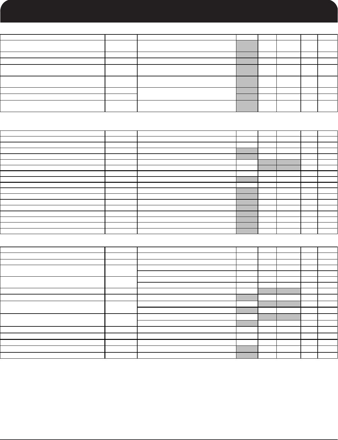
Electrical Characteristics - PCICLK/PCICLK_F
PARAMETER SYMBOL CONDITIONS MIN
TY P
MAX UNITS
NOTES
Output Impedance R
DSP
V
O
= V
DD
*(0.5) 12 55
Ω
1
Long Accuracy ppm see Tperiod min-max values -100 100 ppm 2
33.33MHz output no spread 29.99700 30.00300 ns 2
33.33MHz output spread 30.08421 30.23459 ns 2
33.33MHz output no spread 29.49700 30.50300 ns 2
33.33MHz output nominal/spread 29.56617 30.58421 ns 2
Output High Voltage V
OH
I
OH
= -1 mA 2.4 V
1
Output Low Voltage V
OL
I
OL
= 1 mA 0.4 V 1
V
OH
@MIN = 1.0 V
-33 mA 1
V
OH
@MAX = 3.135 V
-33 mA 1
V
OL
@ MIN = 1. 95 V 30 mA 1
V
OL
@ MAX = 0.4 V
38 mA 1
Rising Edge Slew Rate t
SLR
Measured from 0.8 to 2.0 V 1 1.7 4 V/ns 1
Falling Edge Slew Rate
t
FLR
Measured from 2.0 to 0.8 V 1 1.8 4 V/ns 1
Duty Cycle
d
t1
V
T
= 1.5 V 45 50.6 55
%1
Pin to Pin Skew t
sk ew
V
T
= 1.5 V 250 ps 1
Jitter, Cycle to cycle
t
jcyc-cyc
V
T
= 1.5 V 150 500 ps
1
*T
A
= Tambient ; V
DD
= 3.3 V +/-5%; C
L
=5pF, Rs=22
Ω
(unless specified otherwise)
1
Guaranteed b
desi
n and characterization, not 100% tested in
ro d u ct io n.
2
All Lon
Term Ac c urac
and Clock Period s
ecifications are
uaranteed assumin
that REFOUT is at 14.31818MHz
3
Slew rate emastured through V_swing voltage range centered about differential zero
4
Vcross is defined at the voltage where Clock = Clock#.
5
Only applies to the differential rising edge (Clock rising, Clock# falling.)
I
OH
Output High Current
T
abs
T
period
Output Low Current I
OL
Clock period
Absolute min/max period
6
CPU group skew is nominally 0ps.