LTC1068 Series
1
1068fc
TYPICAL APPLICATION
DESCRIPTION
Clock-Tunable, Quad
Second Order, Filter Building Blocks
The LTC
®
1068 product family consists of four monolithic
clock-tunable filter building blocks. Each product contains
four matched, low noise, high accuracy 2nd order switched-
capacitor filter sections. An external clock tunes the center
frequency of each 2nd order filter section. The LTC1068
products differ only in their clock-to-center frequency
ratio. The clock-to-center frequency ratio is set to 200:1
(LTC1068-200), 100:1 (LTC1068), 50:1 (LTC1068-50) or
25:1 (LTC1068-25). External resistors can modify the clock-
to-center frequency ratio. High performance, quad 2nd
order, dual 4th order or 8th order filters can be designed
with an LTC1068 family product. Designing filters with an
LTC1068 product is fully supported by FilterCAD™ filter
design software for Windows.
The LTC1068 products are available in a 28-pin SSOP
surface mount package. A customized version of an
LTC1068 family product can be obtained in a 16-lead SO
package with internal thin-film resistors. Please contact
LTC Marketing for details.
Gain vs Frequency
FEATURES
APPLICATIONS
n
Four Identical 2nd Order Filter Sections in an
SSOP Package
n
2nd Order Section Center Frequency Error:
±0.3% Typical and ±0.8% Maximum
n
Low Noise per 2nd Order Section, Q ≤ 5:
LTC1068-200 50µV
RMS
, LTC1068 50µV
RMS
LTC1068-50 75µV
RMS
, LTC1068-25 90µV
RMS
n
Low Power Supply Current: 4.5mA, Single 5V,
LTC1068-50
n
Operation with ±5V Power Supply, Single 5V
Supply or Single 3.3V Supply
n
Lowpass or Highpass Filters:
LTC1068-200, 0.5Hz to 25kHz; LTC1068, 1Hz to
50kHz; LTC1068-50, 2Hz to 50kHz; LTC1068-25,
4Hz to 200kHz
n
Bandpass or Bandreject (Notch) Filters:
LTC1068-200, 0.5Hz to 15kHz; LTC1068, 1Hz to
30kHz; LTC1068-50, 2Hz to 30kHz; LTC1068-25,
4Hz to 140kHz
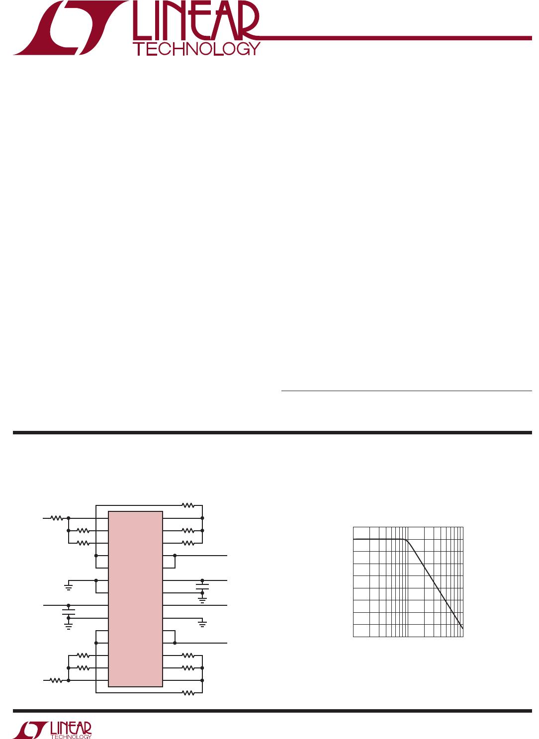
Dual, Matched, 4th Order Butterworth Lowpass Filters, Clock-Tunable Up
to 200kHz f – 3dB = f
CLK
/25, 4th Order Filter Noise = 60µV
RMS
INV B
HPB/NB
BPB
LPB
SB
NC
AGND
V
+
NC
SA
LPA
BPA
HPA/NA
INVA
28
27
26
25
24
23
22
21
20
19
18
17
16
15
1
2
3
4
5
6
7
8
9
10
11
12
13
14
INV C
HPC/NC
BPC
LPC
SC
V
NC
CLK
NC
SD
LPD
BPD
HPD/ND
INVD
LTC1068-25
R31 20k
R33 20k
R23 14k
R13 20k
0.1µF
R21 14k R22 20k
R12 14k
R32 10k
R34 10k
R24 20k
R14 14k
R11 20k
V
IN1
V
IN2
5V
1µF
V
OUT1
V
OUT2
1068 TA01
–5V
f
CLK
= (25)(f – 3dB)
RELATIVE FREQUENCY [f
IN
/(f – 3dB)]
0.1
GAIN (dB)
–10
–20
–30
–40
–50
–60
–70
–80
1 10
1068 TA02
10
0
L, LT, LTC, LTM, Linear Technology and the Linear logo are registered trademarks and
FilterCAD is a trademark of Linear Technology Corporation. All other trademarks are the property
of their respective owners.
LTC1068 Series
2
1068fc
ABSOLUTE MAXIMUM RATINGS
Total Supply Voltage (V
+
to V
) ................................12V
Power Dissipation
.............................................. 500mW
Input Voltage at Any Pin
......V
– 0.3V ≤ V
IN
≤ V
+
+ 0.3V
Storage Temperature Range
...................65°C to 150°C
(Note 1)
1
2
3
4
5
6
7
8
9
10
11
12
13
14
TOP VIEW
G PACKAGE
28-LEAD PLASTIC SSOP
28
27
26
25
24
23
22
21
20
19
18
17
16
15
INV B
HPB/NB
BPB
LPB
SB
NC
AGND
V
+
NC
SA
LPA
BPA
HPA/NA
INV A
INV C
HPC/NC
BPC
LPC
SC
V
NC
CLK
NC
SD
LPD
BPD
HPD/ND
INV D
T
JMAX
= 110°C, θ
JA
= 95°C/W
1
2
3
4
5
6
7
8
9
10
11
12
TOP VIEW
24
23
22
21
20
19
18
17
16
15
14
13
INV B
HPB/NB
BPB
LPB
SB
AGND
V
+
SA
LPA
BPA
HPA/NA
INV A
INV C
HPC/NC
BPC
LPC
SC
V
CLK
SD
LPD
BPD
HPD/ND
INV D
N PACKAGE
24-LEAD PDIP
T
JMAX
= 110°C, θ
JA
= 65°C/W
PIN CONFIGURATION
Operating Temperature Range
LTC1068C ................................................ 0°C to 70°C
LTC1068I.............................................40°C to 85°C
Lead Temperature (Soldering, 10 sec)
.................. 300°C
ORDER INFORMATION
LEAD FREE FINISH TAPE AND REEL PART MARKING PACKAGE DESCRIPTION TEMPERATURE RANGE
LTC1068CG#PBF LTC1068CG#TRPBF LTC1068 28-Lead Plastic SSOP 0°C to 70°C
LTC1068IG#PBF LTC1068IG#TRPBF LTC1068 28-Lead Plastic SSOP –40°C to 85°C
LTC1068-200CG#PBF LTC1068-200CG#TRPBF LTC1068 28-Lead Plastic SSOP 0°C to 70°C
LTC1068-200IG#PBF LTC1068-200IG#TRPBF LTC1068 28-Lead Plastic SSOP –40°C to 85°C
LTC1068-50CG#PBF LTC1068-50CG#TRPBF LTC1068 28-Lead Plastic SSOP 0°C to 70°C
LTC1068-50IG#PBF LTC1068-50IG#TRPBF LTC1068 28-Lead Plastic SSOP –40°C to 85°C
LTC1068-25CG#PBF LTC1068-25CG#TRPBF LTC1068 28-Lead Plastic SSOP 0°C to 70°C
LTC1068-25IG#PBF LTC1068-25IG#TRPBF LTC1068 28-Lead Plastic SSOP –40°C to 85°C
LTC1068CN#PBF NA LTC1068 24-Lead PDIP 0°C to 70°C
LTC1068IN#PBF NA LTC1068 24-Lead PDIP –40°C to 85°C
Consult LTC Marketing for parts specified with wider operating temperature ranges.
Consult LTC Marketing for information on nonstandard lead based finish parts.
For more information on lead free part marking, go to: http://www.linear.com/leadfree/
For more information on tape and reel specifications, go to: http://www.linear.com/tapeandreel/
LTC1068 Series
3
1068fc
PARAMETER CONDITIONS MIN TYP MAX UNITS
Operating Supply Voltage Range 3.14 ±5.5 V
Voltage Swings V
S
= 3.14V, R
L
= 5k (Note 2)
V
S
= 4.75V, R
L
= 5k (Note 3)
V
S
= ±5V, R
L
= 5k
l
l
l
1.2
2.6
±3.4
1.6
3.2
±4.1
V
P-P
V
P-P
V
Output Short-Circuit Current (Source/Sink) V
S
= ±4.75V
V
S
= ±5V
17/6
20/15
mA
mA
DC Open-Loop Gain R
L
= 5k 85 dB
GBW Product V
S
= ±5V 6 MHz
Slew Rate V
S
= ±5V 10 V/µs
Analog Ground Voltage (Note 4) V
S
= 5V, Voltage at AGND 2.5V ±2% V
PARAMETER CONDITIONS MIN TYP MAX UNITS
Clock-to-Center Frequency Ratio
(Note 5) V
S
= 4.75V, f
CLK
= 1MHz, Mode 1 (Note 3),
f
O
= 10kHz, Q = 5, V
IN
= 0.5V
RMS
,
R1 = R3 = 49.9k, R2 = 10k
l
100 ±0.3 100 ±0.8
100 ±0.9
%
%
V
S
= ±5V, f
CLK
= 1MHz, Mode 1,
f
O
= 10kHz, Q = 5, V
IN
= 1V
RMS
,
R1 = R3 = 49.9k, R2 = 10k
l
100 ±0.3 100 ±0.8
100 ±0.9
%
%
Clock-to-Center Frequency Ratio,
Side-to-Side Matching (Note 5)
V
S
= 4.75V, f
CLK
= 1MHz, Q = 5 (Note 3)
V
S
= ±5V, f
CLK
= 1MHz, Q = 5
l
l
±0.25
±0.25
±0.9
±0.9
%
%
Q Accuracy (Note 5) V
S
= 4.75V, f
CLK
= 1MHz, Q = 5 (Note 3)
V
S
= ±5V, f
CLK
= 1MHz, Q = 5
l
l
±1
±1
±3
±3
%
%
f
O
Temperature Coefficient ±1 ppm/°C
Q Temperature Coefficient ±5 ppm/°C
DC Offset Voltage (Note 5)
(See Table 1)
V
S
= ±5V, f
CLK
= 1MHz, V
OS1
(DC Offset of Input Inverter)
l
0 ±15 mV
V
S
= ±5V, f
CLK
= 1MHz, V
OS2
(DC Offset of First Integrator)
l
±2 ±25 mV
V
S
= ±5V, f
CLK
= 1MHz, V
OS3
(DC Offset of Second Integrator)
l
±5 ±40 mV
Clock Feedthrough V
S
= ±5V, f
CLK
= 1MHz 0.1 mV
RMS
Max Clock Frequency (Note 6) V
S
= ±5V, Q ≤ 2.0, Mode 1 5.6 MHz
Power Supply Current V
S
= 3.14V, f
CLK
= 1MHz (Note 2)
V
S
= 4.75V, f
CLK
= 1MHz (Note 3)
V
S
= ±5V, f
CLK
= 1MHz
l
l
l
3.5
6.5
9.5
8
11
15
mA
mA
mA
ELECTRICAL CHARACTERISTICS
LTC1068 (Internal Op Amps). The l denotes the specifications which apply
over the full operating temperature range, otherwise specifications are at V
S
= ±5V, T
A
= 25°V, unless otherwise noted.
LTC1068 (Complete Filter) V
S
= ±5V, T
A
= 25°V, unless otherwise noted.

LTC1068-200IG#PBF

Mfr. #:
Manufacturer:
Analog Devices Inc.
Description:
Active Filter Quad Universal Filter Building Block
Lifecycle:
New from this manufacturer.
Delivery:
DHL FedEx Ups TNT EMS
Payment:
T/T Paypal Visa MoneyGram Western Union