LTC1068 Series
30
1068fc
Linear Technology Corporation
1630 McCarthy Blvd., Milpitas, CA 95035-7417
(408) 432-1900
●
FAX: (408) 434-0507
●
www.linear.com
LINEAR TECHNOLOGY CORPORATION 1996
LT 1012 REV C • PRINTED IN USA
RELATED PARTS
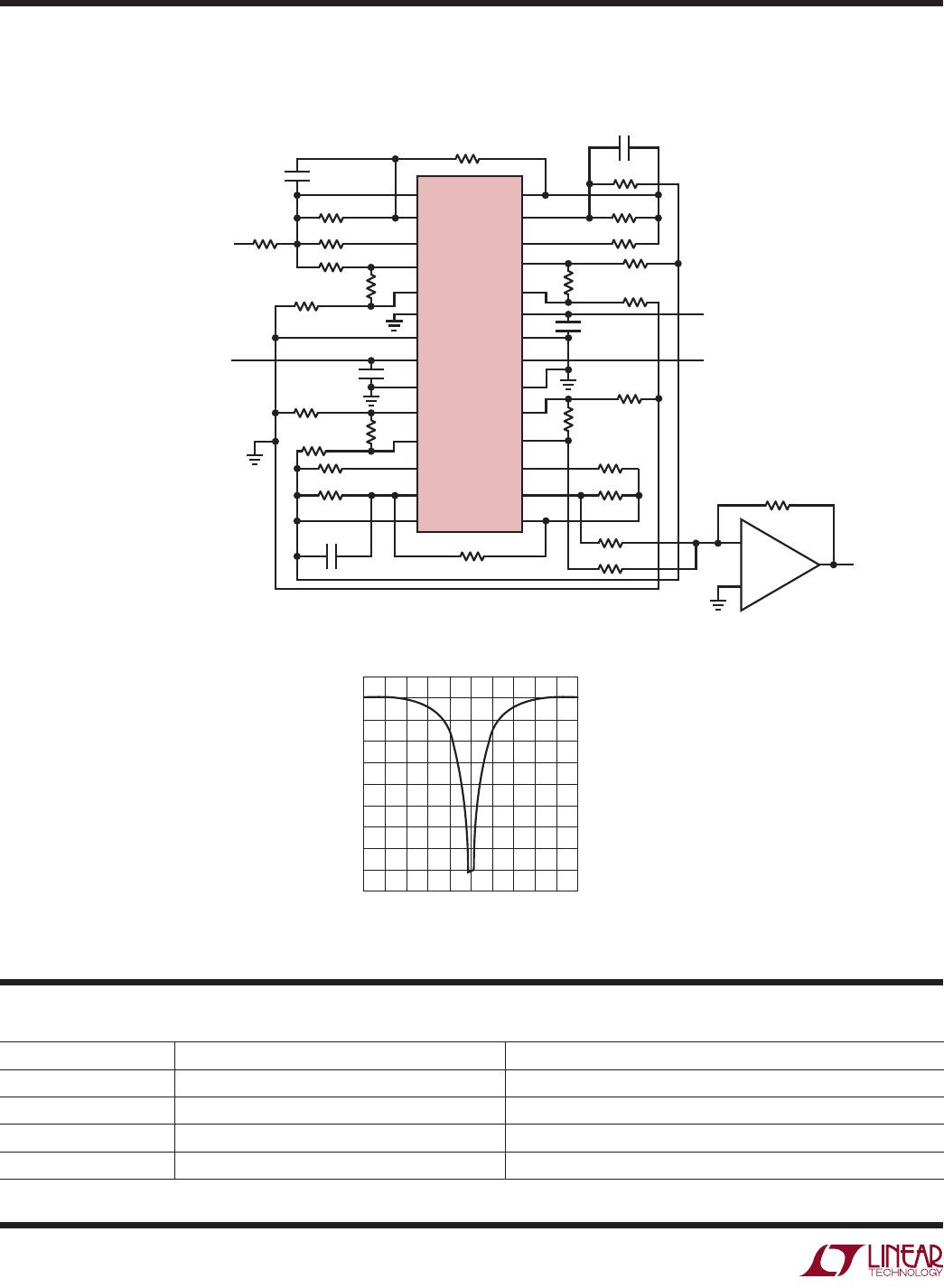
TYPICAL APPLICATION
PART NUMBER DESCRIPTION COMMENTS
LTC1064 Universal Filter, Quad 2nd Order 50:1 and 100:1 Clock-to-f
O
Ratios, f
O
to 100kHz, V
S
= Up to ±7.5V
LTC1067/LTC1067-50 Low Power, Dual 2nd Order Rail-to-Rail, V
S
= 3V to ±5V
LTC1164 Low Power Universal Filter, Quad 2nd Order 50:1 and 100:1 Clock-to-f
O
Ratios, f
O
to 20kHz, V
S
= Up to ±7.5V
LTC1264 High Speed Universal Filter, Quad 2nd Order 20:1 Clock-to-f
O
Ratio, f
O
to 200kHz, V
S
= Up to ±7.5V
LTC1068-200 8th Order Notch, f
NOTCH
= f
CLK
/256, f – 3dB at (0.9) (f
NOTCH
) and (1.05)(f
NOTCH
),
Attenuation at f
NOTCH
Greater Than 70dB for f
NOTCH
in the Frequency Range 200Hz to 5kHz
Gain vs Frequency
INV B
INV C
281
HPB/NB
HPB/NC
272
SB
NC
NC
SC
245
R21 5.11k
R22 6.34k
BPB BPC
263
R31 51.1k
R41 100k
R32 84.3k
LPA LPD
209
R63
8.06k
BPA BPD
1910
R43
178k
C23 470pF
R34 75k
HPA/NA
HPD
1811
INV A
INV D
17
16
15
12
13
14
R33 124k
R23 10k
R24 7.32k
R
H4
5.11k
R
L4
475k
LPB
LPC
25
4
R51
5.11k
R
H2
5.11k
R11 51.1k
V
IN
R64 7.87k
R
G
15k
R62 5.76k
R
L2
66.5k
R
H1
5.11k
R
H3
5.11k
AGND
V
–
236
V
+
227
SA
SD
NC
NC
CLK
218
5V
–5V
f
CLK
= (256)(f
NOTCH
)
V
OUT
1068 TA27
LTC1068-200
0.1µF
C21
470pF
0.1µF
R53
5.11k
R54
5.11k
R52
5.11k
R61
8.06k
C22 470pF
–
+
LT1354
RELATIVE FREQUENCY (f
IN
/f
NOTCH
)
GAIN (dB)
–30
–10
10
1.1
1068 TA28
–50
–70
–40
–20
0
–60
–80
–90
0.8
0.9
1.0
1.2