LTC1068 Series
12
1068fc
MODES OF OPERATION
Linear Technology’s universal switched-capacitor filters
are designed for a fixed internal, nominal f
CLK
/f
O
ratio. The
f
CLK
/f
O
ratio is 100 for the LTC1068, 200 for the LTC1068-
200, 50 for the LTC1068-50 and 25 for the LTC1068-25.
Filter designs often require the f
CLK
/f
O
ratio of each section
to be different from the nominal ratio and in most cases
different from each other. Ratios other than the nominal
value are possible with external resistors. Operating modes
use external resistors, connected in different arrangements
to realize different f
CLK
/f
O
ratios. By choosing the proper
mode, the f
CLK
/f
O
ratio can be increased or decreased from
the part’s nominal ratio.
The choice of operating mode also effects the transfer
function at the HP/N pins. The LP and BP pins always give
the lowpass and bandpass transfer functions respectively,
regardless of the mode utilized. The HP/N pins have a
different transfer function depending on the mode used.
Mode 1 yields a notch transfer function. Mode 3 yields a
highpass transfer function. Mode 2 yields a highpass notch
transfer function (i.e., a highpass with a stopband notch).
More complex transfer functions, such as lowpass notch,
allpass or complex zeros, are achieved by summing two
or more of the LP, BP or HP/N outputs. This is illustrated
in sections Mode 2n and Mode 3a.
Choosing the proper mode(s) for a particular application
is not trivial and involves much more than just adjusting
the f
CLK
/f
O
ratio. Listed here are four of the nearly twenty
modes available. To make the design process simpler and
quicker, Linear Technology has developed the FilterCAD
for Widows design software. FilterCAD is an easy-to-use,
powerful and interactive filter design program. The de-
signer can enter a few filter specifications and the program
produces a full schematic. FilterCAD allows the designer
to concentrate on the filter’s transfer function and not get
bogged down in the details of the design. Alternatively,
those who have experience with the Linear Technology
family of parts can control all of the details themselves.
For a complete listing of all the operating modes, consult
the appendices of the FilterCAD manual or the Help files
in FilterCAD. FilterCAD can be obtained free of charge on
the Linear Technology web site (www.linear.com) or you
can order the FilterCAD CD-ROM by contacting Linear
Technology Marketing.
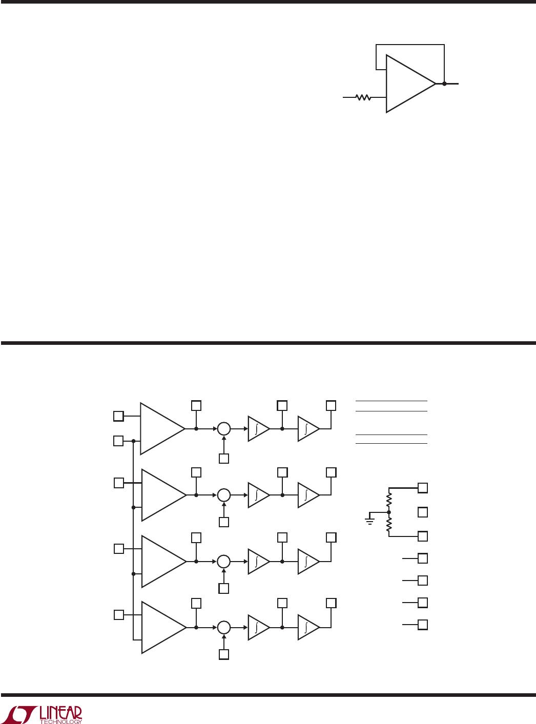
Mode 1
In Mode 1, the ratio of the external clock frequency to
the center frequency of each 2nd order section is inter-
nally fixed at the part’s nominal ratio. Figure 4 illustrates
Mode 1 providing 2nd order notch, lowpass and band-
pass outputs. Mode 1 can be used to make high order
Butterworth lowpass filters; it can also be used to make
low Q notches and for cascading 2nd order bandpass
functions tuned at the same center frequency. Mode 1 is
faster than Mode 3.
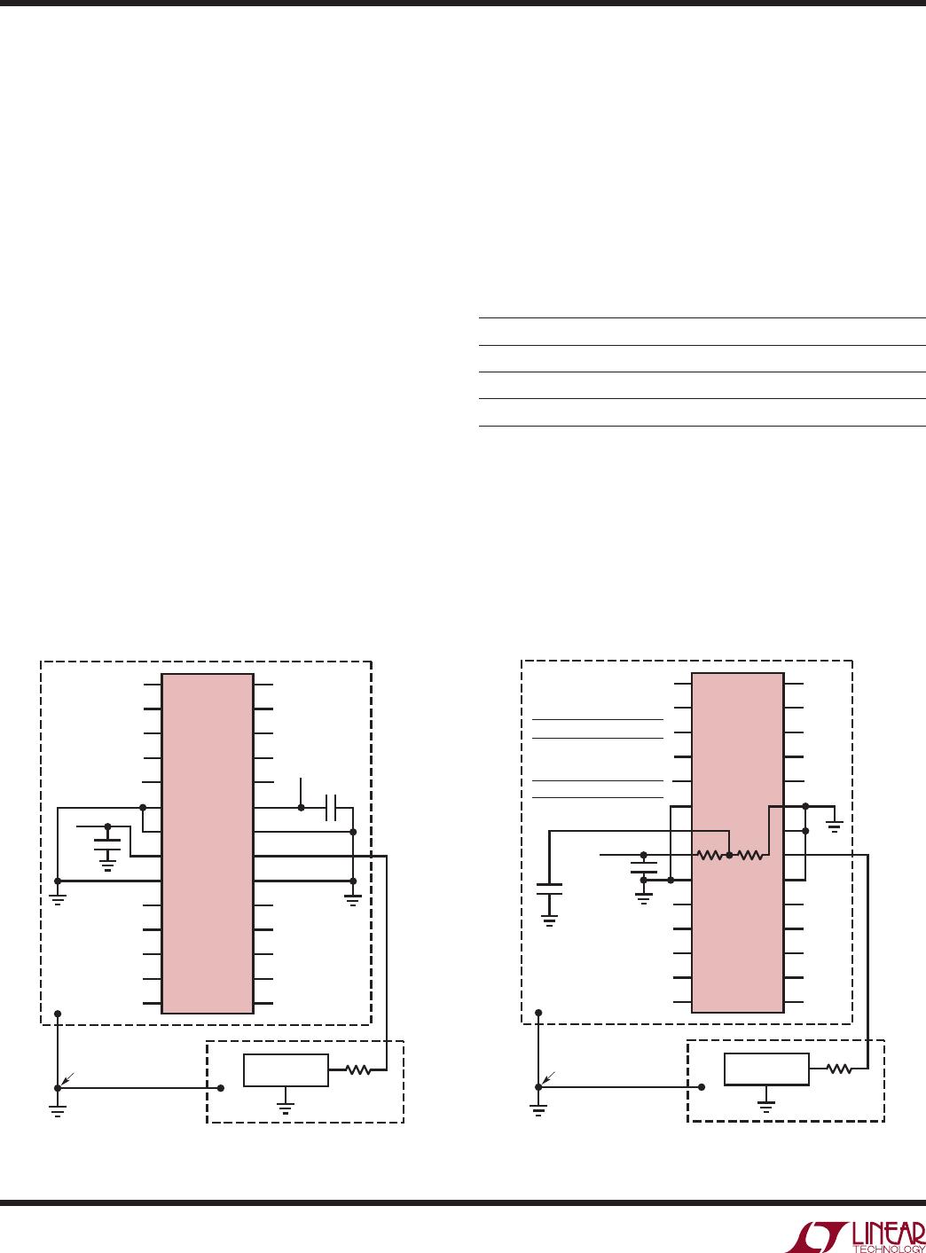
Please refer to the Operating Limits paragraph under Applica-
tions Information for a guide to the use of capacitor C
C
.
Mode 1b
Mode 1b is derived from Mode 1. In Mode 1b (Figure 5)
two additional resistors R5 and R6 are added to lower the
amount of voltage fed back from the lowpass output into
the input of the SA (or SB) switched-capacitor summer.
This allows the filter’s clock-to-center frequency ratio to
be adjusted beyond the part’s nominal ratio. Mode 1b
maintains the speed advantages of Mode 1 and should
be considered an optimum mode for high Q designs with
f
CLK
to f
CUTOFF
(or f
CENTER
) ratios greater than the part’s
nominal ratio.
The parallel combination of R5 and R6 should be kept
below 5k.
Please refer to the Operating Limits paragraph under Applica-
tions Information for a guide to the use of capacitor C
C
.
Figure 4. Mode 1, 2nd Order Filter Providing Notch,
Bandpassing and Lowpass Outputs
–
+
Σ
AGND
R1
N
BP
LP
V
IN
1068 F04
+
–
S
R2
R3
C
C
f
O
= ; f
n
= f
O
Q = ; H
ON
= – ; H
OBP
= –
H
OLP
= H
ON
R2
R1
R3
R1
R3
R2
f
CLK
RATIO
DEVICE
LTC1068
LTC1068-200
LTC1068-50
LTC1068-25
RATIO
100
200
50
25