LTC1068 Series
14
1068fc
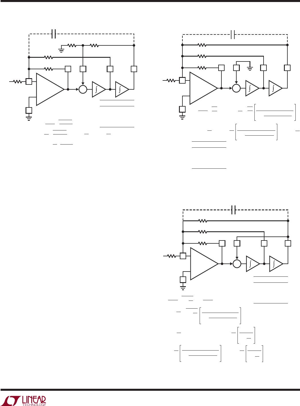
Operating Limits
The Maximum Q vs Center Frequency (f
O
) graphs, under
Typical Performance Characteristics, define an upper
limit of operating Q for each LTC1068 device 2nd order
section. These graphs indicate the power supply, f
O
and
Q value conditions under which a filter implemented with
an LTC1068 device will remain stable when operated at
temperatures of 70°C or less. For a 2nd order section, a
bandpass gain error of 3dB or less is arbitrarily defined
as a condition for stability.
When the passband gain error begins to exceed 1dB, the
use of capacitor C
C
will reduce the gain error (capacitor C
C
is connected from the lowpass node to the inverting node
of a 2nd order section). Please refer to Figures 4 through 7.
The value of C
C
can be best determined experimentally,
and as a guide it should be about 5pF for each 1dB of
gain error and not to exceed 15pF. When operating an
LTC1068 device near the limits defined by the Maximum Q
vs Frequency graphs, passband gain variations of 2dB or
more should be expected.
Clock Feedthrough
Clock feedthrough is defined as the RMS value of the
clock frequency and its harmonics that are present at the
filter’s output pins. The clock feedthrough is tested with
the filter’s input grounded and depends on PC board layout
and on the value of the power supplies. With proper layout
techniques, the typical values of clock feedthrough are
listed under Electrical Characteristics.
Any parasitic switching transients during the rising and
falling edges of the incoming clock are not part of the clock
feedthrough specifications. Switching transients have fre-
quency contents much higher than the applied clock; their
amplitude strongly depends on scope probing techniques
as well as grounding and power supply bypassing. The
clock feedthrough, can be greatly reduced by adding a
simple RC lowpass network at the final filter output. This
RC will completely eliminate any switching transients.
Wideband Noise
The wideband noise of the filter is the total RMS value of
the device’s noise spectral density and is used to determine
APPLICATIONS INFORMATION
the operating signal-to-noise ratio. Most of its frequency
contents lie within the filter passband and cannot be
reduced with post filtering. For a notch filter the noise of
the filter is centered at the notch frequency.
The total wideband noise (µV
RMS
) is nearly independent
of the value of the clock. The clock feedthrough specifica-
tions are not part of the wideband noise.
For a specific filter design, the total noise depends on the
Q of each section and the cascade sequence. Please refer
to the Noise vs Q graphs under the Typical Performance
Characteristics.
Aliasing
Aliasing is an inherent phenomenon of switched-capacitor
filters and occurs when the frequency of the input signals
that produce the strongest aliased components have a
frequency, f
IN
, such as (f
SAMPLING
– f
IN
) that falls into the
filter’s passband. For an LTC1068 device the sampling
frequency is twice f
CLK
. If the input signal spectrum is
not band-limited, aliasing may occur.
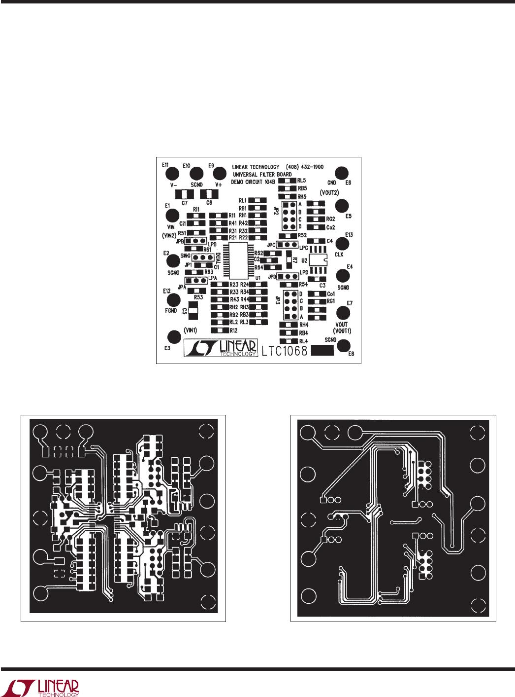
Demonstration Circuit 104
DC104 is a surface mount printed circuit board for the
evaluation of Linear Technology’s LTC1068 product family
in a 28-lead SSOP package. The LTC1068 product family
consists of four monolithic clock-tunable filter building
blocks.
Demo Board 104 is available in four assembled versions:
Assembly 104-A features the low noise LTC1068CG (clock-
to-center frequency ratio = 100), assembly 104-B features
the low noise LTC1068-200CG (clock-to-center frequency
ratio = 200), assembly 104-C features the high frequency
LTC1068-25CG (clock-to-center frequency ratio = 25) and
assembly 104-D features the low power LTC1068-50CG
(clock-to-center frequency ratio = 50).
All DC104 boards are assembled with input, output and
power supply test terminals, a 28-lead SSOP filter device
(LTC1068CG Series), a dual op amp in an SO-8 for input
or output buffers and decoupling capacitors for the filter
and op amps. The filter and dual op amps share the power