Valley Current Mode Control Buck Converter
A4403
10
Allegro MicroSystems, LLC
115 Northeast Cutoff
Worcester, Massachusetts 01615-0036 U.S.A.
1.508.853.5000; www.allegromicro.com
The amount of capacitance required for a given ripple voltage can
be found:
C
IN
=
.
I
rms
× T
on
V
RIPPLE
(15)
As mentioned in the previous section, E-field biasing effects
can reduce the actual capacitance and this should be taken into
account when making the selection.
Again, there is generally no need to consider the heating effects
of the RMS current flowing through the ESR of a ceramic
capacitor. If an electrolytic device is used, then the ripple current
rating should be considered. Note that most manufacturers only
consider the RMS current rating at 100 kHz.
Recirculation Diode This diode (D1) conducts during the
switch off-time. A Schottky diode is recommended to minimize
both the forward drop and switching losses. The worst-case
dissipation occurs at maximum V
IN
, when the duty cycle is at a
minimum.
The average current through the diode can be found:
I
DIODE(av)
= I
LOAD
× (1 – D (min)) . (16)
The forward voltage drop, V
f
, can be found from the diode
characteristics by using the actual load current (not the average
current).
The static power dissipation can be found:
P
STAT
= I
DIODE(av)
× V
f
. (17)
It is also important to take into account the thermal rating of
the package, R
θJA
, and the ambient temperature, to ensure that
enough heatsinking is provided to maintain the diode junction
temperature within the safe operating area for the device.
To minimize the heating effects from the A4403 on the diode and
vice-versa, it is recommended that the diode be mounted on the
reverse side of the printed circuit board.
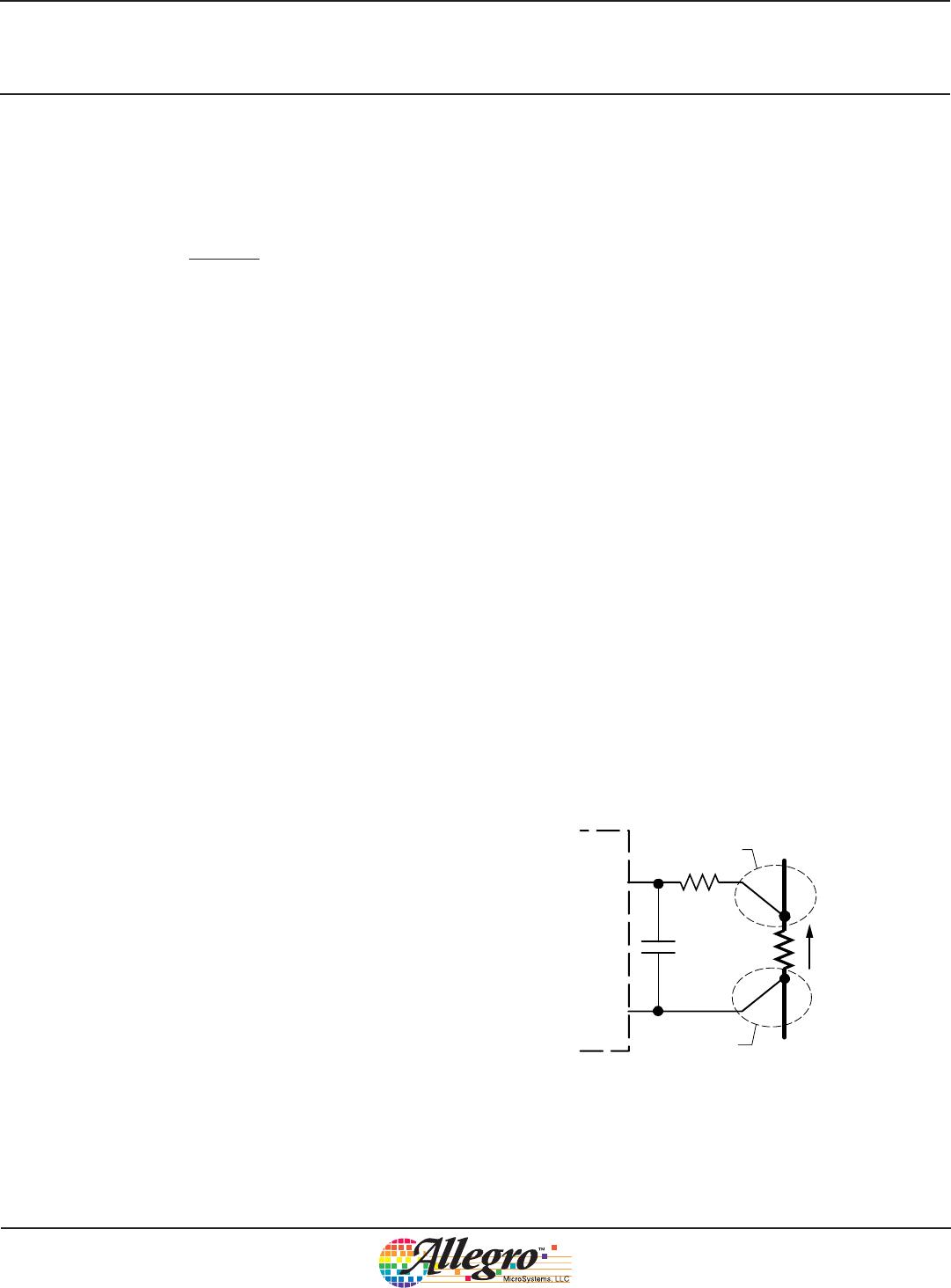
Sense Resistor The sense resistor should be a surface mount
package, with low inductance. On no account should a wire-
wound or through hole package be used. To prevent potential
mistriggering problems from occurring in noisy systems, it is
recommended that an R-C filter be applied across the sense resis-
tor, as shown in figure 3.
The sense resistor value is selected depending on the maximum
output load current. The typical sense voltage that causes a cur-
rent limit is 180 mV. So, for example, a 50 m value would be
appropriate for a maximum load of 3 A, as it allows for margin
between maximum load and the current limit. A tolerance of up to
±5% is acceptable.
The power rating of the resistor has to be considered. The current
flowing in the resistor is essentially the same as the current flow-
ing through the recirculation diode, although the power dissipa-
tion is worked out using the RMS current.
To a first approximation, the sense resistor dissipation can be
worked out as:
P
SENSE
= I
LOAD
2
× (1 – D (min)) × R
SENSE
. (18)
For a converter working with a load of 3 A, a very narrow duty
cycle, and a sense resistor of 50 m, the power dissipation would
be 450 mW.
The optimal solution from a cost perspective is to use two
100 m, 1206-style resistors connected in parallel. Each resistor
is generally rated at 250 mW at 70°C ambient. Check the vendor
datasheet to verify the maximum ambient at full power.
When laying out the PCB, it is essential that the sense resistor
connections, carrying the power current (see figure 3), are as
short and wide as possible to minimize the effects of leakage
inductance noise. In addition, the Kelvin sense circuit connec-
tions should be as close to the sense resistor pads as possible.
Figure 3. R-C filter added to the current sense circuit
ISEN
Kelvin
connection
Kelvin
connection
A4403
SGND
47
R
FILTER
R
SENSE
Power
current
1 nF
C
FILTER
Valley Current Mode Control Buck Converter
A4403
11
Allegro MicroSystems, LLC
115 Northeast Cutoff
Worcester, Massachusetts 01615-0036 U.S.A.
1.508.853.5000; www.allegromicro.com
R
FILTER
and C
FILTER
(R7 and C7 in the Typical Application
diagram) should be placed close to the A4403 pins. The ground
sense should connect directly to the SGND and not to the power
ground.
Support Components The bootstrap capacitor (C2) and soft-
start capacitor (C5) should be ceramic X5R or X7R.
Thermal Considerations To ensure the A4403 operates in
the safe operating area, which effectively means restricting the
junction temperature to less than 150°C, several checks should be
made. The general approach is to work out what thermal imped-
ance, R
JA
, is required to maintain the junction temperature at
a given level, for a particular power dissipation. (Another factor
worth considering is that other power dissipating components
on the system PCB may influence the thermal performance of
the A4403. For example, the power loss contribution from the
recirculation diode and the sense resistor may cause the junction
temperature of the A4403 to be higher than expected.) It should
be noted that this process is usually an iterative one to achieve the
optimum solution.
The following steps can be used as a guideline for determining
the R
JA
for a suitable thermal solution. :
1. Estimate the maximum ambient temperature, T
A
(max) , of the
application.
2. Define the maximum junction temperature, T
J
(max). Note that
the absolute maximum is 150°C.
3. Determine the worst case power dissipation, P
D
(max). This will
occur at maximum load and minimum V
IN
. Contributors are:
(a) Switch static losses
Estimate the maximum duty cycle:
D (max)
=
,
V
OUT
+ V
f
V
IN
(min) + V
f
(19)
where V
f
is the forward voltage drop of the Schottky diode (D1)
and sense resistor (R2, R3) under the given load current.
Estimate the R
DS(on)
of the buck switch at the given junction
temperature:
R
DS(on)TJ
R
DS(on)25C
1+
=
.
170
T
J
– 25
(20)
The static loss for each switch can be determined:
P
STAT
= I
LOAD
2
× D (max) × R
DS(on)TJ
, (21)
where I
LOAD
is the load.
(b) Switch dynamic losses
Both the turn-on and the turn-off losses can be estimated:
P
DYN
V
IN
(min)
×
×
5
×
10
–9
× f
SW
× 1.6
=
,
I
LOAD
2
(22)
where f
SW
is the switching frequency.
(c) Diode capacitance turn-on loss
At turn-on, an additional current spike flows into the switch, caus-
ing a loss as follows:
P
DIODECAP
=
,
C
DIODE
× V
IN
2
× f
SW
2
(23)
where C
DIODE
is the body capacitance of the Schottky diode (D1).
(d) Control losses
The control losses can be estimated as follows:
P
CTRL
= I
VINON
× V
IN
, (24)
where I
VINON
is the quiescent current with the converter enabled.
(e) Gate charge losses
Estimate the charge losses as follows:
P
GATE
= Q × f
SW
× V
IN
, (25)
where Q = 5 nC and is the charge that is required to turn on the
buck switch.
Valley Current Mode Control Buck Converter
A4403
12
Allegro MicroSystems, LLC
115 Northeast Cutoff
Worcester, Massachusetts 01615-0036 U.S.A.
1.508.853.5000; www.allegromicro.com
(f) The total losses can now be estimated:
P
TOTAL
= P
STAT
+ P
DYN
+ P
DIODECAP
+ P
CTRL
+ P
GATE
. (26)
4. The thermal impedance required for the solution can now be
determined:
R
QJA
=
.
T
J
T
A
P
TOTAL
(27)
Note that if a four-layer high thermal efficiency board is used, a
thermal impedance of around 30°C/W can be achieved.
Example
Given selected parameters:
V
IN
(min) = 42 V,
V
OUT
= 3.3 V at 3 A,
f
SW
= 1 MHz,
T
A
= 70°C,
Target junction temperature, T
J
= 115°C,
V
f
= 0.55 V, and
C
DIODE
= 150 pF, then:
(a) Switch static losses
Maximum duty cycle (equation 19):
D (max) 0.09
==
3.3
+ 0.55
42 + 0.55
R
DS(on)
of the buck switch (equation 20):
R
DS(on)TJ
350 × 10
–3
1+
=
0.535 Ω
=
170
115
– 25
Static loss for each switch (equation 21):
P
STAT
= 3
2
× 0.09 × 0.535 = 0.433 W
(b) Switch dynamic losses (equation 22):
P
DYN
42
×
0.504 W
×
5
×
10
–9
× 1000 × 10
3
×1.6
==
2
3
(c) Diode capacitance turn-on loss (equation 23):
P
DIODECAP
0.132 W
=
1
50
×
10
–12
× 42
2
×1
×
10
6
=
2
(d) Control losses (equation 24):
P
CTRL
= 0.004 × 42 = 0.168 W
(e) Gate charge losses (equation 25):
P
GATE
= 5 × 10
–9
× 1 × 10
6
× 42 = 0.21 W
(f) Total losses (equation 26):
P
TOTAL
= 0.433 + 0.504 + 0.132 + 0.168 + 0.21 = 1.447 W
Thermal impedance (equation 27):
R
QJA
31°C/W
==
115
– 70
1.447
For this particular solution, a PCB with high thermal efficency is
required to ensure the junction temperature is kept below 115°C.
For maximum effectiveness, the PCB area underneath the thermal
pad of the A4403 should be flooded with copper. Several thermal
vias (say between 4 and 8) should be used to connect the thermal
pad to the internal ground plane. If possible, a further thermal
copper plane should be applied to the bottom side of the PCB and
connected to the thermal pad of the A4403 through the vias.
This calculation assumes no thermal influence from other compo-
nents. If possible, it is advisable to mount the recirculation diode
(D1) on the reverse side of the printed circuit board. Ensure low
impedance electrical connections are implemented between board
layers.
PCB Layout Guidelines The ground plane is largely dic-
tated by the thermal requirements of the previous section. The
ground-referenced power components should be referenced to a
star ground, located away from the A4403 to minimize ground
bounce issues.
A small, local, relatively quiet ground plane near the A4403
should be used for the ground-referenced support components,
to minimize interference effects of ground noise from the power
circuitry. Figure 4 illustrates the recommended grounding archi-
tecture.

APEK4403GEU-01-T-DK

Mfr. #:
Manufacturer:
Description:
BOARD EVAL FOR A4403
Lifecycle:
New from this manufacturer.
Delivery:
DHL FedEx Ups TNT EMS
Payment:
T/T Paypal Visa MoneyGram Western Union

Products related to this Datasheet