Valley Current Mode Control Buck Converter
A4403
13
Allegro MicroSystems, LLC
115 Northeast Cutoff
Worcester, Massachusetts 01615-0036 U.S.A.
1.508.853.5000; www.allegromicro.com
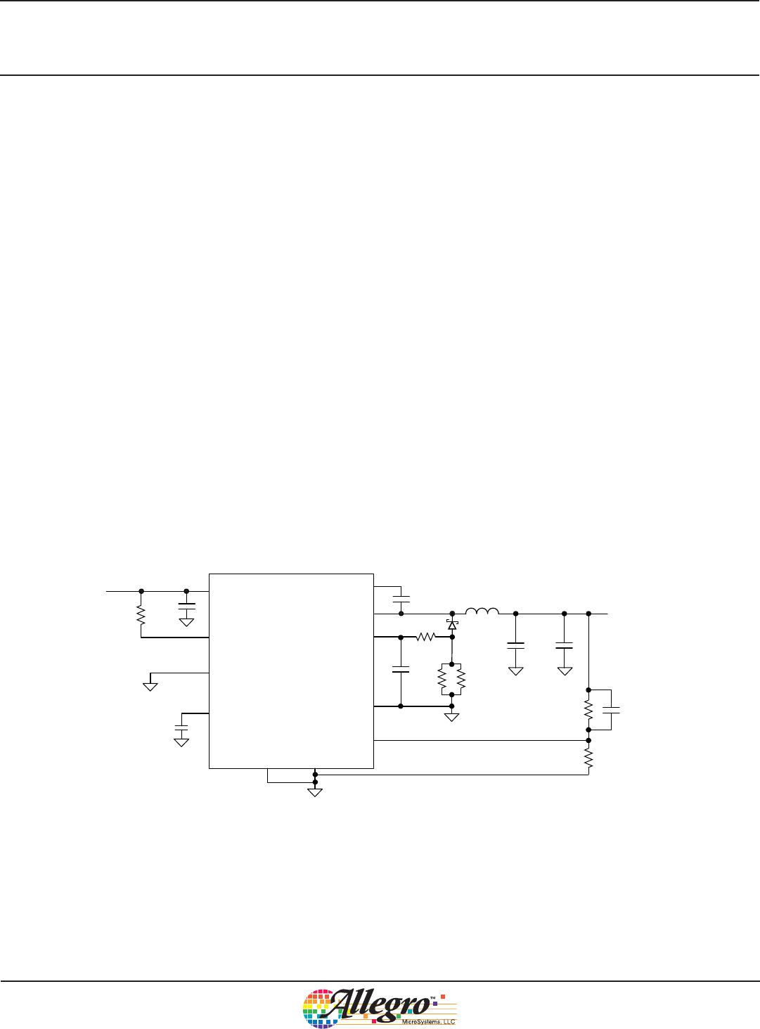
To avoid ground offset issues in the output voltage, it is highly
recommended that the ground-referenced feedback resistor R6
should be connected directly to the GND connection of the
A4403. In other words, the R6 ground return should avoid the use
of the internal ground plane.
All ground-referenced support components (C5 and the DIS
switch) should also be located as close to the GND connection as
possible. A “local quiet” ground plane around these components
can be implemented; however, this ground plane should have a
high impedance connection to the star ground connection of the
power stages, as referenced below.
The sense resistor connections should be connected in a Kelvin
circuit (see figure 3) to the corresponding pins on the A4403
(ISEN and SGND). Note that it is imperative that the PCB traces
between the sense resistor pads and the sense connections are as
short as possible to minimize the effects of leakage inductance.
In noisy systems, it is highly recommended that an R-C filter be
used to filter the signal produced across the ISEN pin. See the
Sense Resistor section and the Typical Application schematic.
If an internal ground plane is used, it is recommended that it
does not overlap the switching node, LX, to avoid the possibility
of noise pick up. To minimize the possibility of noise injection
issues, it is recommended to isolate the ground plane around the
high impedance nodes, such as FB and SS.
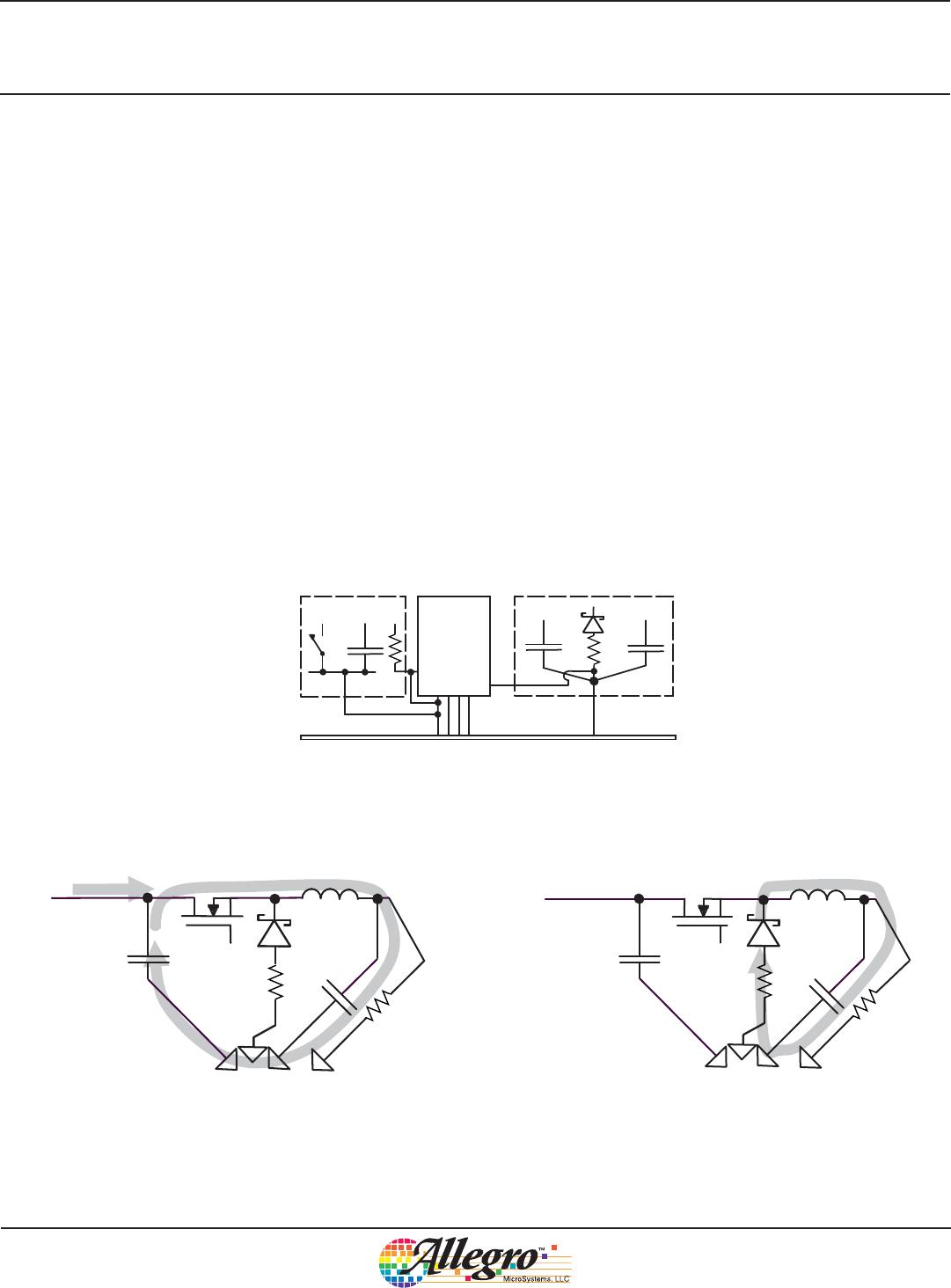
Q
L
R
LOAD
VIN
V
OUT
D
C
OUT
C
IN
LX
Star Connection
R
Input
Voltage
Figure 5. FET on-cycle current conduction paths
Q
L
VIN
LX
Star Connection
D
R
Input
Voltage
R
LOAD
V
OUT
C
OUT
C
IN
Figure 6. FET off-cycle current conduction paths
Cin
Cout
D
Star Connection
A4403
Internal Ground Plane
Thermal Vias
Power Circuitry
A4403 Support
Com
p
onents
Local ‘quiet’
Ground Plane
GND
R
R6
Switch
C5
SGND
Figure 4. Ground plane configurations
Valley Current Mode Control Buck Converter
A4403
14
Allegro MicroSystems, LLC
115 Northeast Cutoff
Worcester, Massachusetts 01615-0036 U.S.A.
1.508.853.5000; www.allegromicro.com
In terms of grounding the power components, a star connection
should be made to minimize the ground loop impedances. Note
that, although a ground plane may be required to meet the ther-
mal characteristics of the solution, it is still imperative to imple-
ment a star ground connection for the power components.
Figures 5 and 6 illustrate the importance of keeping the ground
connections as short as possible and forming good star connec-
tions.
Figure 5 also illustrates the current conduction paths during the
on-cycle of the switching FET. The following points should be
noted:
• The capacitor C
IN
should be placed as close as possible to the
VIN terminal.
• The inductor L should placed as close as possible to the LX
terminal and to the output capacitors C
OUT
.
• Good separation should exist between the LX connection and
any adjacent components or traces.
Figure 6 shows the current conduction path during the off-cycle
of the switching FET. The following points should be noted:
• The diode D should be placed as close as possible to both the
switching FET and to the inductor. The resistor R should be
placed as close as possible to the diode D.
• The boostrap capacitor, C2, and the soft start capacitor, C5,
should be located as close as possible to their respective termi-
nal connections. The ground reference of the soft start capacitor
should be connected as close to the GND terminal as possible.
GNDNC
L
D1
1
6.3 H
LX
FB
VIN
5.0 V
3 A
6.3 V
ISEN
SGND
V
OUT
A 4403
TON
22 nF
R1
100 k
C1
2.2 F
100 V
100 m
SS
DIS
R3
47
R2
750
R6
3.92 k
R5
100 m
R4
C2
10 nF
C6
47 nF
C5
10 F
C3
1 nF
C7
6.3 V
10 F
C4
BOOT
V
IN
9 to 46 V
Switching Frequency = 1 MHz
All capacitors are X5R or X7R ceramic
Resistors R3 and R4 should be surface mount, low inductance type, rated at 250 mW at 70°C
Figure 7. Typical application
Valley Current Mode Control Buck Converter
A4403
15
Allegro MicroSystems, LLC
115 Northeast Cutoff
Worcester, Massachusetts 01615-0036 U.S.A.
1.508.853.5000; www.allegromicro.com
Package EU, 16-Contact QFN
0.95
C
SEATING
PLANE
C0.08
17X
16
16
2
1
1
2
16
2
1
A
A
Terminal #1 mark area
Coplanarity includes exposed thermal pad and terminals
B
Exposed thermal pad (reference only, terminal #1
identifier appearance at supplier discretion)
For Reference Only
(reference JEDEC MO-220WGGC)
Dimensions in millimeters
Exact case and lead configuration at supplier discretion within limits shown
C
D
D
C
Reference land pattern layout (reference IPC7351
QFN65P400X400X80-17W2M)
All pads a minimum of 0.20 mm from all adjacent pads; adjust as necessary
to meet application process requirements and PCB layout tolerances; when
mounting on a multilayer PCB, thermal vias at the exposed thermal pad land
can improve thermal dissipation (reference EIA/JEDEC Standard JESD51-5)
4.10
0.35
0.65
4.10
0.65
0.75 ±0.050.30 ±0.05
0.40 ±0.10
2.70
2.70
4.00 ±0.15
4.00 ±0.15
2.70
2.70
B
PCB Layout Reference View

APEK4403GEU-01-T-DK

Mfr. #:
Manufacturer:
Description:
BOARD EVAL FOR A4403
Lifecycle:
New from this manufacturer.
Delivery:
DHL FedEx Ups TNT EMS
Payment:
T/T Paypal Visa MoneyGram Western Union

Products related to this Datasheet