Valley Current Mode Control Buck Converter
A4403
4
Allegro MicroSystems, LLC
115 Northeast Cutoff
Worcester, Massachusetts 01615-0036 U.S.A.
1.508.853.5000; www.allegromicro.com
ELECTRICAL CHARACTERISTICS
1
valid at T
J
= 25°C, V
IN
= 9 to 46 V, unless otherwise noted
Characteristic Symbol Conditions Min. Typ. Max. Units
General
V
IN
Quiescent Current
I
VINOFF
DIS = high, VIN = 46 V 100 A
I
VINON
DIS = low, VIN = 46 V, I
LOAD
= 1 mA 4.3 5.5 mA
Feedback Voltage V
FB
T
J
= 25°C 0.792 0.8 0.808 V
Feedback Input Bias Current I
BIAS
–400 –100 100 nA
Output Voltage Tolerance
2
V
OUT
I
LOAD
= 1 mA to 3 A –2.5 2.5 %
On-Time Tolerance T
ON
Based on selected value –15 15 %
Minimum On-Time Period T
on(min)
50 60 ns
Minimum Off-Time Period T
off(min)
350 ns
Buck Switch On-Resistance R
DS(on)
T
J
= 25°C, I
LOAD
= 3 A 350 m
T
J
= 125°C, I
LOAD
= 3 A 550 m
Current Limit Threshold I
LIM
Valley current in external sense resistors = 50 m 3.0 3.6 4.2 A
Soft Start Current Source I
SS
5 10 15 A
Input
DIS Input Voltage Threshold V
DIS
Device enabled 1 V
DIS Open-Circuit Voltage V
DISOC
Device disabled 2 7 V
DIS Input Current I
IN
DIS = 0 V –10 –1 A
Protection
FB Overvoltage Shutdown V
FBOV
0.88 – V
VIN Undervoltage Shutdown Threshold V
INUV
Voltage rising 6.4 7.5 V
VIN Undervoltage Shutdown Hysteresis V
INUV(hys)
0.7 1.1 V
Overtemperature Shutdown Threshold T
JTSD
Temperature rising – 165 – °C
Overtemperature Shutdown Hysteresis T
JTSD(hys)
Recovery = T
JTSD
– T
JTSD(hys)
15 °C
1
Specifications over the junction temperature range of –40°C to 125°C are assured by design and characterization.
2
Average value of V
OUT
relative to target voltage. Note that the tolerance effects of the feedback resistors are not taken into account. This figure does
include the feedback voltage tolerance.
Valley Current Mode Control Buck Converter
A4403
5
Allegro MicroSystems, LLC
115 Northeast Cutoff
Worcester, Massachusetts 01615-0036 U.S.A.
1.508.853.5000; www.allegromicro.com
Basic Operation The A4403 is a buck converter that utilizes
valley current-mode control. The on-time is set by the amount
of current that flows into the TON pin. This is determined by the
value of the TON resistors chosen (R1 and R2 in the Functional
Block diagram) and the magnitude of the input voltage, V
IN
.
Under a specific set of conditions, an on-time can be set that
then dictates the switching frequency. This switching frequency
remains reasonably constant throughout load and line conditions
as the on-time varies inversely with the input voltage. The Switch
On-Time and Switching Frequency section provides more details
on this subject.
At the beginning of the switching cycle, the buck switch is turned
on for a fixed period that is determined by the current flowing
into TON. Once the current comparator trips, a one-shot mono-
stable, the On Timer, is reset, turning off the switch. The current
through the inductor then decays. This current is sensed through
the external sense resistors (R3 and R4), and then compared
against the current-demand signal. The current-demand signal is
generated by comparing the output voltage against an accurate
bandgap reference. After the current through the sense resistors
decreases to the valley of the current-demand signal, the On
Timer is set to turn the buck switch back on again and the cycle is
repeated.
Under light load conditions, the converter automatically operates
in pulse frequency modulation (PFM) mode to maintain regu-
lation. This mode of operation ensures optimum efficiency as
switching losses are reduced.
Overcurrent Protection The converter utilizes pulse-by-pulse
valley current limiting, which operates when the current through
the sense resistors, R3 and R4 (set for 50 m by two 100 m
resistors in parallel), increases above 3.6 A typical at the valley
point. The corresponding sense voltage (at the ISEN pin) that cre-
ates a current limiting condition is 180 mV typical. It is possible,
by careful selection of the sense resistors, to reduce the current
limit for systems with maximum loads of less than 3 A.
During an overload condition, the switch is turned on for the
period determined by the constant on-time circuitry. The switch
off-time is extended until the current decays to the current limit
value of 3.6 A typical (which corresponds to a sense voltage of
180 mV). The switch is then turned on again.
Because no slope compensation is required in this control
scheme, the current limit is maintained at a reasonably constant
level across the input voltage range.
Figure 1 illustrates how the current is limited during an overload
condition. The current decay (period with switch off) is propor-
tional to the output voltage. As the overload is increased, the out-
put voltage tends to decrease and the switching period increases.
Output Voltage Selection The output voltage of the converter
is set by selecting the appropriate feedback resistors, using the
following formula:
R
5
R
6
=,
V
FB
V
OUT
1
(1)
where (refering to the Functional Block diagram):
R
6
has a value between 750 and 12 k (R6 connected between
the GND and FB pins),
R
5
is the dependent value (R5 connected between the output rail
and the FB pin),
V
OUT
is the user-configured output regulator voltage, and
V
FB
is the reference voltage.
The tolerance of the feedback resistors influences the voltage set-
point. It is therefore important to consider the tolerance selection
when targeting an overall regulation figure.
Functional Description
Current Limit level
Inductor current operating at maximum load
Maximum load
Constant On-Time
Constant On-Time
CurrentCurrent
Time
Constant period
Current Limit level
Inductor current operating in a “soft” overload
Overload
Time
Extended period
Figure 1. Current limiting during overload
Valley Current Mode Control Buck Converter
A4403
6
Allegro MicroSystems, LLC
115 Northeast Cutoff
Worcester, Massachusetts 01615-0036 U.S.A.
1.508.853.5000; www.allegromicro.com
In general, the feedback resistors should have the lowest resis-
tance possible, to minimize any noise pick-up effects and to
minimize voltage offsets on the output caused by the bias current,
I
BIAS
, flowing out of the FB node into R6. Reducing the feedback
resistances does introduce another loading effect on the output,
which has an effect on the standby current.
It should be noted that a minimum load of 1 mA is required (see
the Light Load Operation section). This may be provided by the
feedback resistors. For example, if R6 = 750 , this guarantees a
1 mA load current.
Disable The converter is enabled by pulling the DIS pin low.
Once enabled, the output converter is started-up under the control
of the soft-start routine.
To disable the converter, the DIS pin can simply be disconnected
(open circuit).
Soft Start A soft-start routine is initiated when: DIS = 0, no
thermal shutdown exists, and V
IN
and the internal housekeeping
supplies are above the minimum values. Note that an overcurrent
event does not initiate a soft start, unless the converter is recover-
ing from a thermal shutdown condition.
The soft-start routine controls the rate of rise of the reference
voltage, which in turn controls the output voltage. This function
minimizes the amount of inrush current drawn from VIN and
potential voltage overshoot on the output rail, VOUT.
The soft-start period, T
SS
, is set by an internal current source
that charges the external capacitor (C5) connected to the SS pin.
Control by the soft-start routine is completed when the SS pin
reaches 0.8 V. The duration of T
SS
is set by selecting the appro-
priate capacitance, according to the formula:
T
SS
=.
10
×10
–6
C
5
× 0.8
(2)
Note: If the soft start function is not required for the application,
a 220 k resistor should be connected between the SS pin and
GND. Without soft start, or with a soft start period that is too
rapid, coupled with a high load that is present during start-up, the
converter may operate in current limit, placing maximum stress
on the input circuit.
Assuming no load is drawn until the start-up process is complete,
the current drawn from the input supply is determined by how
quickly the output capacitors (C3 and C4) are charged. The out-
put capacitors are charged according to the following formula:
t
CHARGE
=,
I
V
IN
C
OUT
× V
OUT
(3)
where I
VIN
is the input supply current.
For example, if you limited I
VIN
to 250 mA, and assumed V
OUT
=
5 V and C
OUT
= 20 F, the soft start time could be determined as:
t
CHARGE
==
0.25 A
20 μF × 5 V
400 μs
This means a soft-start duration greater than 400 s should be
selected to ensure the inrush current is less than 250 mA.
Shutdown The converter is disabled in the event of either an
overtemperature event, or an undervoltage on VIN (V
INUVR
) or
on an internal housekeeping supply.
As soon as any of the above faults have been removed and
assuming DIS = 0, the output voltage, V
OUT
, is brought-up under
the control of the soft-start routine.
Output Overvoltage Protection In the event of an over-
voltage condition appearing on the output rail, the FB terminal
will also experience the overvoltage, scaled by the feedback resis-
tors. If the FB terminal voltage rises above the nominal voltage
by 10% (typical), the on-time of the buck switch will terminate
and the switch will remain off until the FB voltage reduces to the
correct V
FB
range.
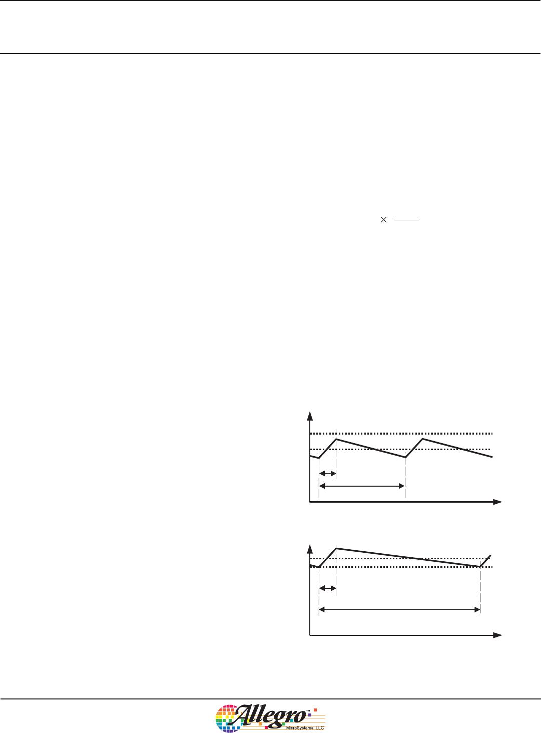
Switch On-Time and Switching Frequency The switch
on-time effectively determines the operating frequency of the
converter. The selection of the operating frequency is generally
a trade-off between the size of the external passive components
(inductor, and input and output capacitors) and switching losses.
Another consideration in selecting the switching frequency is to
ensure that none of the on- or off-time limits are reached under
extreme conditions.
The minimum on-time occurs at maximum input voltage and
minimum load. Consider the following example.
Given:
V
IN
(max) = 46 V, V
OUT
= 5 V, f
SW
= 1 MHz, and:
T
on
(min)
=
,
V
IN
+ V
f
V
OUT
+ V
f
f
SW
1
×
(4)
where V
f
is the voltage drop of the recirculation diode (D1) and
sense resistors (R3 and R4).

APEK4403GEU-01-T-DK

Mfr. #:
Manufacturer:
Description:
BOARD EVAL FOR A4403
Lifecycle:
New from this manufacturer.
Delivery:
DHL FedEx Ups TNT EMS
Payment:
T/T Paypal Visa MoneyGram Western Union

Products related to this Datasheet