Valley Current Mode Control Buck Converter
A4403
7
Allegro MicroSystems, LLC
115 Northeast Cutoff
Worcester, Massachusetts 01615-0036 U.S.A.
1.508.853.5000; www.allegromicro.com
Then, the minimum on-time is:
T
on
(min)
118 ns
==
46 + 0.5
5 + 0.5
1
×
1× 10
6
The specified minimum on-time, T
on(min)
, is 60 ns maximum, so
there is reasonable margin in this case.
The specified minimum off-time, T
off(min)
, 350 ns maximum,
also has to be considered. The minimum off-time occurs at
minimum input voltage and maximum load. As was shown in the
minimum on-time calculation (equation 4), you have to exam-
ine the extreme operating conditions to ensure adequate margin
exists.
The switch on-time, T
on
, is set by the current flowing into the
TON pin. The current is determined by the input voltage, V
IN
,
and the resistor R1. The on-time can be found as:
T
on
=
.
V
IN
× 2.05
×10
10
R
1
+ 10
×
10
–9
(5)
The switching frequency may be slightly modulated by load
changes. The on-time is always constant for a given input voltage
and across the load range. To compensate for any losses in the
circuitry (for example, in the series switch and inductor, or in the
voltage drop across the recirculation diode), the off-time, hence
the switching frequency, has to be adjusted. This effect is most
noticeable at low input voltages and high output currents.
To calculate the actual switching frequency, the T
on
of equa-
tion 5 can be used in conjunction with the transfer function of the
converter:
f
SW
=
.
V
IN
+
V
f
V
OUT
+
V
f
T
on
1
×
(6)
An alternative approach to selecting the TON resistor (R1), to
accomplish an approximate switching frequency is found in the
following formula:
R
1
=
.
f
SW
V
OUT
× 2.05
× 10
10
(7)
Figure 2 illustrates a range of switching frequencies that can be
achieved with various TON resistances and output voltages.
Top-Off Charge Pump During light load operation, when
operating in PFM mode, the top-off charge pump provides
enough charge to drive the buck switch.
Light Load Operation To avoid the output voltage peak charg-
ing due to leakage effects from the buck switch and the charge
pump recirculation current, a minimum load of 1 mA must be
applied to the output.
The output feedback resistor network provides some loading.
Depending on the values selected, this network may provide all,
or at least some, of the minimum loading requirement.
Control Loop The process of closing the control loop for the
A4403 has been greatly simplified through the integration of
the compensation components into the device. The control loop
bandwidth has been optimized for operation across the full input
and output voltage range and for switching frequencies between
450 kHz and 2 MHz. Loop optimization is achieved with a 20 F
ceramic capacitor placed across the output (VOUT to GND) and
a power inductor that achieves a peak to peak ripple current of
around 720 mA. For example, for a 3.3 V output operating at a
frequency of 1 MHz, the power inductor = 4.7 H.
Larger output capacitors can be used; however, this tends to
decrease the bandwidth of the control loop. Note that the output
capacitance should not exceed 1000 F or be less than 10 F, as
this may cause a loop instability to occur.
400
600
800
1000
1200
1400
1600
1800
2000
10 100 1000
Resistor R1 (kΩ)
Switching Frequency (kHz)
0.8 V 1.5 V 3.3 V 5 V 12 V
V
OUT
Figure 2. Switching frequencies versus TON resistor values, at various
levels of V
OUT
Valley Current Mode Control Buck Converter
A4403
8
Allegro MicroSystems, LLC
115 Northeast Cutoff
Worcester, Massachusetts 01615-0036 U.S.A.
1.508.853.5000; www.allegromicro.com
When the output voltage is set for 0.8 V, the typical bandwidth
is 90 kHz with a phase margin of 45° at full load. As the load is
reduced, the bandwidth remains largely constant; however, the
phase margin tends to reduce slightly because the output power
pole is shifted down in frequency, introducing the phase lag
sooner. At light loads, before pulse frequency modulation occurs,
the phase margin reduces to approximately 40°, which is reason-
able given that it is the worst-case condition. Note that when
pulse frequency modulation occurs, the system no longer operates
as a linear system, therefore, the control laws do not apply.
When the output voltage is set for higher voltages, the DC gain
is reduced by the resistor feedback network from the output. This
effectively reduces the bandwidth of the control loop. An optional
speed-up capacitor (C6) can be used in parallel with the feedback
resistor (R5) to compensate for this effect. The addition of this
capacitor introduces an additional zero which increases the gain
and extends the bandwidth to maintain it in the region of 90 kHz.
The position of the zero depends on the values of R5 and C6.
The following time constants should be used for various output
voltages:
Output Voltage
(V)
Time Constant
(τ)
5 3.6 × 10
–5
3.3 2.4 × 10
–5
2.5 1.8 × 10
–5
1.5 1.1 × 10
–5
0.8 Not required
For example, assume a target output voltage of 5 V, and an R5
of 3.92 k to achieve that voltage. Then C6 = 9.18 × 10
–9
. The
nearest commonly available value is 10 nF.
For applications that require output voltages (V
OUT
) other than
what is defined above, the following formula should be used to
calculate the time constant:
τ = V
OUT
× 7.2 × 10
–6
, (8)
Inductor The main factor in selecting the inductance value is
the ripple current. The ripple current affects the output voltage
ripple and also has an effect on the current limit. Because slope
compensation is not used, the ripple current is not constrained by
this factor.
A good starting point in selecting the inductance for a given
application is to specify a maximum peak-to-peak ripple current
of about 25% of the maximum load. The equates to a ripple cur-
rent of approximately 750 mA for a maximum load of 3 A. This
often gives a good compromise between size, cost, and perfor-
mance.
The maximum peak to peak ripple current, I
RIPP
, occurs at the
maximum input voltage. Therefore the duty cycle, D, should be
found under these conditions:
D (min)
=
,
V
OUT
+V
f
V
IN
(max)+V
f
(9)
where V
f
is the forward voltage drop of the recirculation diode
and the sense resistor.
The required inductance can be found:
L
(min)
D (min)
=
.
I
RIPP
V
IN
V
OUT
f
SW
(min)
1
××
(10)
Note that the manufacturers inductance tolerance should also be
taken into account. This value may be as high as ±20%.
In addition, because the control is dependant on the valley signal,
it is important to consider the minimum peak to peak valley
voltage that is developed across the sense resistor. The minimum
peak to peak ripple current occurs at minimum input voltage. The
peak to peak voltage is simply the peak to peak current multiplied
by the sense resistor value. It is recommended that the peak to
peak sense voltage should be greater than 25 mV.
It is recommended that gapped ferrite solutions be used as
opposed to powdered iron solutions. The latter exhibit relatively
high core losses that can have a large impact on long term reli-
ability.
Inductors are typically specified at two current levels:
• RMS current. It is important to understand how the RMS cur-
rent level is specified, in terms of ambient temperature. Some
manufacturers quote an ambient only, whilst others quote a tem-
perature that includes a self-temperature rise. For example, if an
inductor is rated for 85°C and includes a self-temperature rise of
25°C at maximum load, then the inductor cannot be safely oper-
ated beyond an ambient temperature of 60°C at full load. The
RMS current can be assumed to be simply the maximum load
Valley Current Mode Control Buck Converter
A4403
9
Allegro MicroSystems, LLC
115 Northeast Cutoff
Worcester, Massachusetts 01615-0036 U.S.A.
1.508.853.5000; www.allegromicro.com
current, with perhaps some margin to allow for overloads, and
so forth.
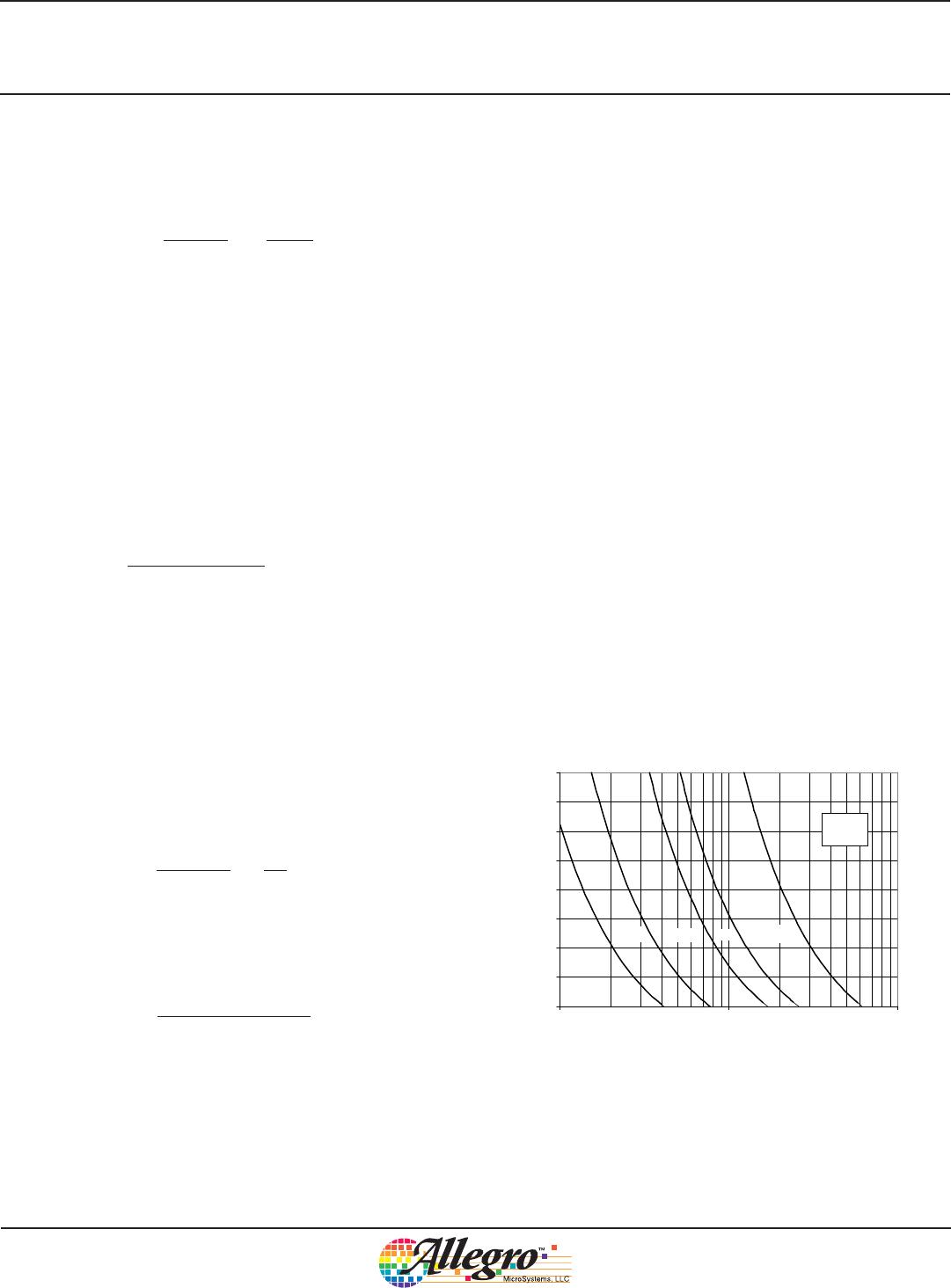
• saturation current. The worst case maximum peak current
should not exceed the saturation current and indeed some mar-
gin should be allowed. The maximum peak current can be found
to ensure the saturation current level of the chosen inductor is
not exceeded:
I
sat
I
LOAD
+
=
.
I
RIPPLE
2
(11)
It is important to ensure that, under worst-case conditions (mini-
mum input voltage, maximum load current, minimum inductance,
and minimum switching frequency), that the minimum current
limit is not exceeded and in fact has some margin. The current
limit is measured at the valley level. The maximum current at the
valley is found from:
I
valley
I
LOAD
=
.
I
RIPPLE
2
(12)
The minimum current limit threshold should be at least 20%
above this level.
Recommended inductor manufacturers and ranges are:
• Tayo Yuden: NR6045 series
• Sumida: CDR7D43MN series
Output Capacitor In the interests of size, cost, and perfor-
mance, this control architecture has been designed for ceramic
capacitors. It is imperative that ceramic X5R or X7R capacitors
are used. On no account should Y5V, Y5U, Z5U, or similar types
be used.
When using ceramic capacitors, another important consider-
ation is the E-field effects on the actual value of the capacitor.
To minimize the effects of the capacitance being reduced with
output voltage, it is recommended that the working voltage of the
capacitor be considerably more than the set output voltage. Check
with the vendor to obtain this information.
The output capacitor determines the output voltage ripple and is
used to close the control loop. As outlined in the Control Loop
section, the bandwidth has been optimized for an output capaci-
tance of 20 F.
If a particular application requires an extremely low output volt-
age, the output capacitor can be increased. Any increase will tend
to reduce the bandwidth and therefore compromise the transient
response performance.
In general the output capacitance should not exceed 1000 F or
be less than 10 F, as this may cause a loop instability to occur.
The output ripple is largely determined by the output capacitance,
and the effects of ESR and ESL can largely be ignored assum-
ing good layout practice is observed. To help reduce the effects
of ESL it is a good idea to split the 20 F capacitance into two
separate 10 F components.
The output voltage ripple can be approximated to:
V
RIPPLE
,
I
RIPPLE
8 × f
SW
× C
OUT
(13)
where I
RIPPLE
is as found in the Inductor section.
When using ceramic capacitors, due to the negligible heating
effects of the ESR, there is generally no need to consider the cur-
rent carrying capability. Also, the RMS current flowing into the
output capacitor is extremely low.
Input Capacitor It is recommended that ceramic X5R or X7R
capacitors be used, or at least that they be used in conjunction
with some other capacitor technology; for example, aluminum
electrolytic. Note that the self-resonance of electrolytics tend to
occur in the 100s of kHz, therefore the effects of ESL become
apparent at switching frequencies in the region of 1 MHz.
The value of the input capacitance determines the amount of
ripple voltage that appears at the source terminals. If a system is
designed correctly, the input capacitor should supply the switch-
ing current minus the input average current during the on-time of
the power switch. During the off-time of the power switch, the
input capacitor is charged-up.
The RMS current that flows in the input capacitor can be found
from:
I
rms
1
=
,
I
OUT
× V
OUT
×
V
IN
V
OUT
V
IN
1/2
(14)
The amount of ripple voltage that appears across the input termi-
nals depends on: the amount of charge removed during the switch
on-time and the actual capacitor value. If a capacitor technology
such as an electrolytic is used, then the effects of ESR also have
to be considered.

APEK4403GEU-01-T-DK

Mfr. #:
Manufacturer:
Description:
BOARD EVAL FOR A4403
Lifecycle:
New from this manufacturer.
Delivery:
DHL FedEx Ups TNT EMS
Payment:
T/T Paypal Visa MoneyGram Western Union

Products related to this Datasheet