Si824x
10 Preliminary Rev. 0.3
Table 5. IEC 60747-5-2 Insulation Characteristics*
Parameter Symbol Test Condition
Characteristic
Unit
NB SOIC-16
Maximum Working Insulation Voltage
V
IORM
560 V peak
Input to Output Test Voltage
V
PR
Method b1
(V
IORM
x1.875=V
PR
,
100%
Production Test, t
m
= 1 sec,
Partial Discharge < 5 pC)
1050 V peak
Transient Overvoltage
V
IOTM
t = 60 sec 4000 V peak
Pollution Degree
(DIN VDE 0110, Table 1)
2
Insulation Resistance at T
S
,
V
IO
=500V
R
S
>10
9
*Note: Maintenance of the safety data is ensured by protective circuits. The Si824x provides a climate classification of
40/125/21.
Table 6. IEC Safety Limiting Values
1
Parameter
Symbol Test Condition NB SOIC-16 Unit
Case Temperature
T
S
150 °C
Safety Input Current
I
S
JA
= 105 °C/W (NB SOIC-16),
V
DDI
=5.5V,
V
DDA
=V
DDB
=24V,
T
J
= 150 °C, T
A
=2C
50 mA
Device Power Dissipation
2
P
D
1.2 W
Notes:
1. Maximum value allowed in the event of a failure. Refer to the thermal derating curve in Figure 5.
2. The Si82xx is tested with V
DDI
=5.5V, V
DDA
=V
DDB
=24V, T
J
=15C, C
L
= 100 pF, input 2 MHz 50% duty cycle
square wave.
Si824x
Preliminary Rev. 0.3 11
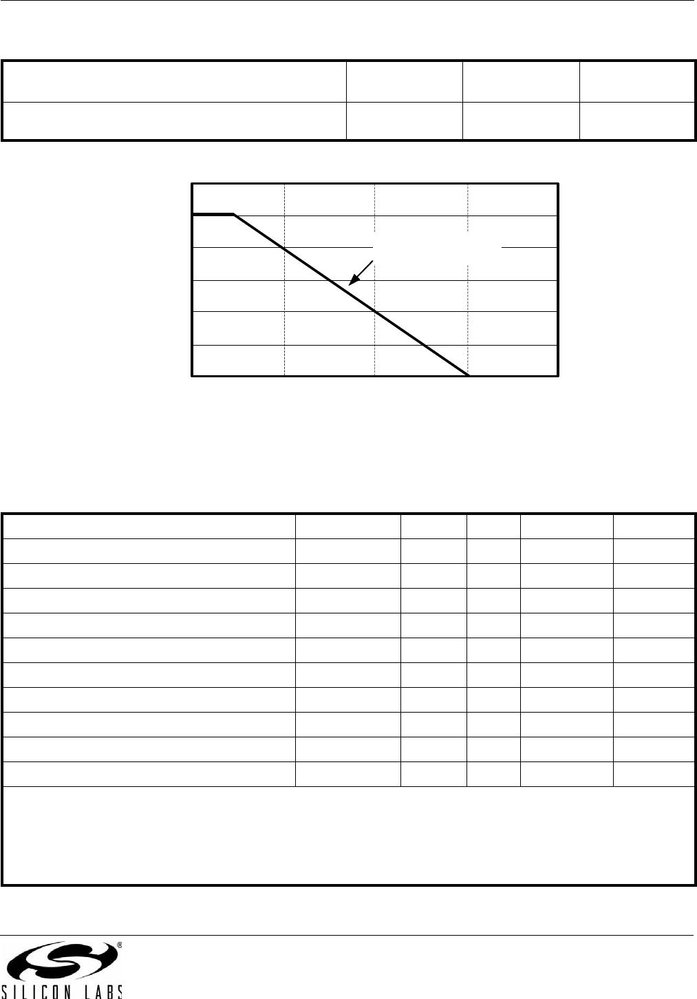
Figure 5. NB SOIC-16, Thermal Derating Curve, Dependence of Safety Limiting Values with Case
Temperature per DIN EN 60747-5-2
Table 7. Thermal Characteristics
Parameter
Symbol
NB
SOIC-16
Unit
IC Junction-to-Air
Thermal Resistance
JA
105 °C/W
Table 8. Absolute Maximum Ratings
1
Parameter Symbol Min Typ Max Units
Storage Temperature
2
T
STG
–65 +150 °C
Ambient Temperature under Bias T
A
–40 +125 °C
Input-side Supply Voltage VDDI –0.6 6.0 V
Driver-side Supply Voltage VDDA, VDDB –0.6 30 V
Voltage on any Pin with respect to Ground VIN –0.5 VDD + 0.5 V
Output Drive Current per Channel I
O
—— 10 mA
Lead Solder Temperature (10 sec) 260 °C
Latchup Immunity
3
—— 100 V/ns
Maximum Isolation (Input to Output) 2500 V
RMS
Maximum Isolation (Output to Output) 1500 V
RMS
Notes:
1. Permanent device damage may occur if the absolute maximum ratings are exceeded. Functional operation should be
restricted to the conditions as specified in the operational sections of this data sheet. Exposure to absolute maximum
rating conditions for extended periods may affect device reliability.
2. VDE certifies storage temperature from –40 to 150 °C.
3. Latchup immunity specification is for slew rate applied across GNDI and GNDA or GNDB.
0 20015010050
60
40
20
0
Case Temperature (ºC)
Safety-Limiting Current (mA)
VDDI = 5.5 V
VDDA, VDDB = 24 V
10
30
50
Si824x
12 Preliminary Rev. 0.3
3. Functional Description
The operation of an Si824x channel is analogous to that of an opto coupler and gate driver, except an RF carrier is
modulated instead of light. This simple architecture provides a robust isolated data path and requires no special
considerations or initialization at start-up. A simplified block diagram for a single Si824x channel is shown in
Figure 6.
Figure 6. Simplified Channel Diagram
A channel consists of an RF Transmitter and RF Receiver separated by a semiconductor-based isolation barrier.
Referring to the Transmitter, input A modulates the carrier provided by an RF oscillator using on/off keying. The
Receiver contains a demodulator that decodes the input state according to its RF energy content and applies the
result to output B via the output driver. This RF on/off keying scheme is superior to pulse code schemes as it
provides best-in-class noise immunity, low power consumption, and better immunity to magnetic fields. See
Figure 7 for more details.
Figure 7. Modulation Scheme
RF Oscillator
Modulator Demodulator
A
B
Semiconductor-
Based Isolation
Barrier
Transmitter Receiver
Dead
Time
Generator
0.5 to 4 A
peak
Gnd
V
DD
Driver
Input Signal
Output Signal
Modulation Signal

SI8244CB-D-IS1

Mfr. #:
Manufacturer:
Silicon Labs
Description:
Gate Drivers 2.5kV 4A Class D Audio Driver, 10V UVLO PWM input
Lifecycle:
New from this manufacturer.
Delivery:
DHL FedEx Ups TNT EMS
Payment:
T/T Paypal Visa MoneyGram Western Union