Si824x
Preliminary Rev. 0.3 7
2.1. Test Circuits
Figures 2 and 3 depict sink current and source current test circuits.
Figure 2. IOL Sink Current Test Circuit
Figure 3. IOH Source Current Test Circuit
INPUT
1 µF
100 µF
10
RSNS
0.1
Si824x
1 µF
CER
10 µF
EL
VDDA = VDDB = 15 V
IN OUT
VSS
VDD
SCHOTTKY
50 ns
200 ns
Meas ure
INPUT WAVEFORM
GND
VDDI
VDDI
8 V
+
_
INPUT
1 µF
100 µF
10
RSNS
0.1
Si824x
1 µF
CER
10 µF
EL
VDDA = VDDB = 15 V
IN OUT
VSS
VDD
50 ns
200 ns
Meas ure
INPUT WAVEFORM
GND
VDDI
SCHOTTKY
VDDI
5.5 V
+
_
Si824x
8 Preliminary Rev. 0.3
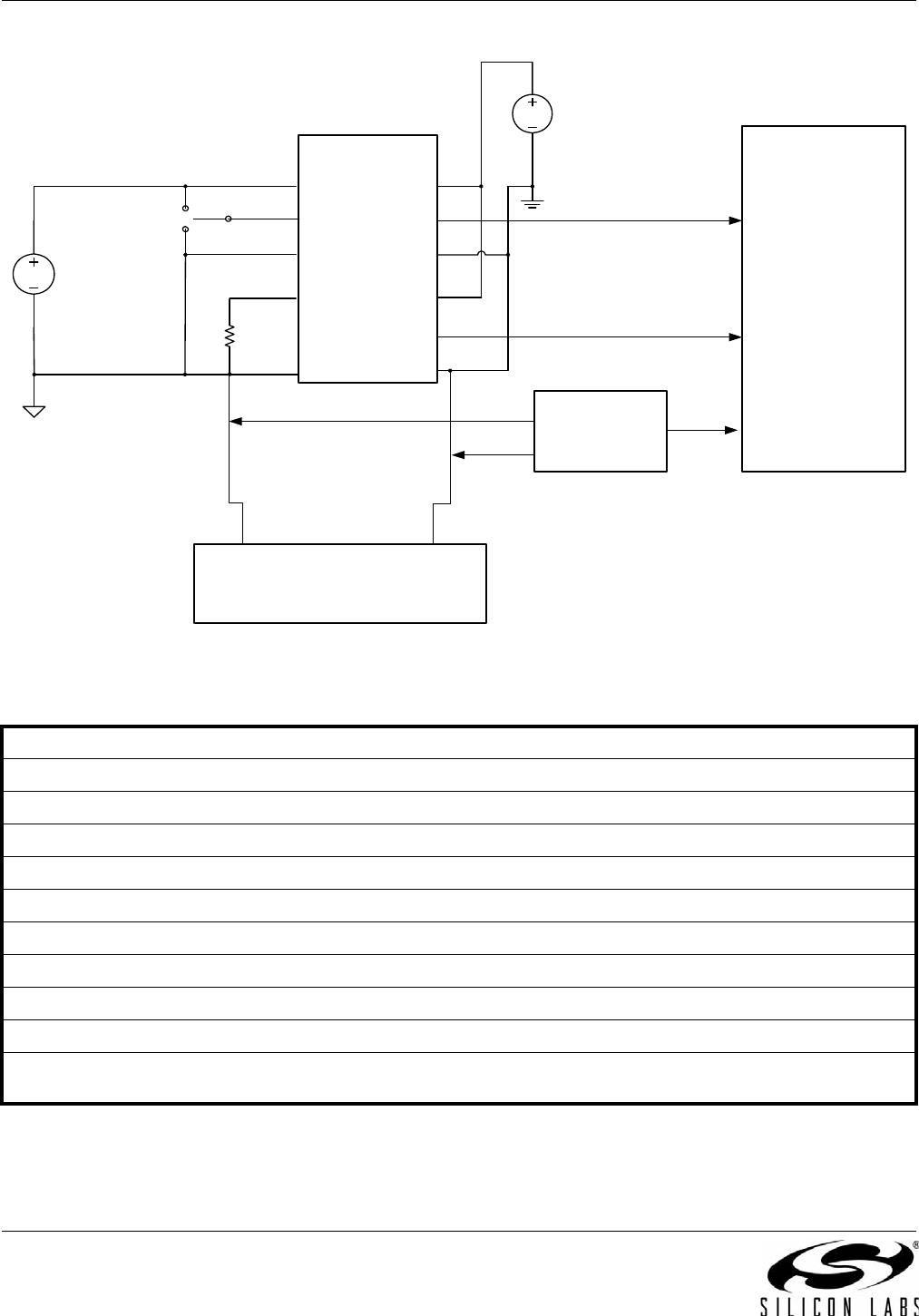
Figure 4. Common Mode Transient Immunity Test Circuit
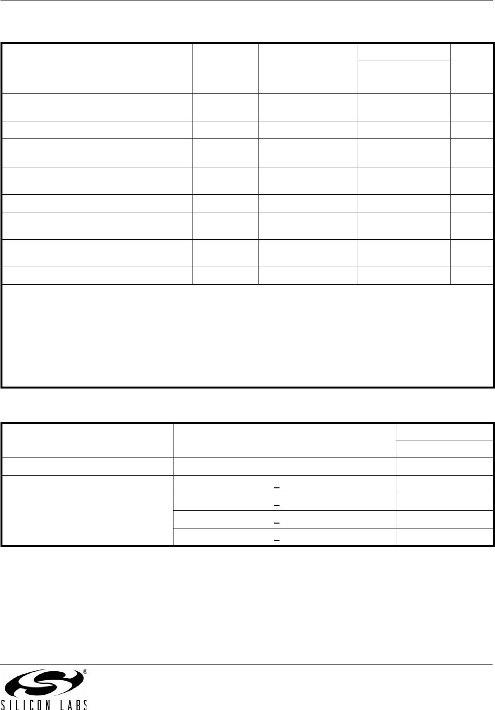
Table 2. Regulatory Information*
CSA
The Si824x is certified under CSA Component Acceptance Notice 5A. For more details, see File 232873.
61010-1: Up to 300 V
RMS
reinforced insulation working voltage; up to 600 V
RMS
basic insulation working voltage.
60950-1: Up to 300 V
RMS
reinforced insulation working voltage; up to 600 V
RMS
basic insulation working voltage.
VDE
The Si824x is certified according to IEC 60747-5-2. For more details, see File 5006301-4880-0001.
60747-5-2: Up to 560 V
peak
for basic insulation working voltage.
UL
The Si824x is certified under UL1577 component recognition program. For more details, see File E257455.
Rated up to 2500 V
RMS
isolation voltage for basic protection.
*Note: Regulatory Certifications apply to 2.5 kV
RMS
rated devices, which are production tested to 3.0 kV
RMS
for 1 sec.
For more information, see "6.Ordering Guide" on page 26.
Si824x
Preliminary Rev. 0.3 9
Table 3. Insulation and Safety-Related Specifications
Parameter Symbol Test Condition
Value
Unit
NBSOIC-16
2.5 kV
RMS
Nominal Air Gap
(Clearance)
1
L(1O1) 4.01 mm
Nominal External Tracking (Creepage)
1
L(1O2) 4.01 mm
Minimum Internal Gap
(Internal Clearance)
0.011 mm
Tracking Resistance
(Proof Tracking Index)
PTI IEC60112 600 V
Erosion Depth
ED 0.019 mm
Resistance
(Input-Output)
2
R
IO
10
12
Capacitance
(Input-Output)
2
C
IO
f=1MHz 1.4 pF
Input Capacitance
3
C
I
4.0 pF
Notes:
1. The values in this table correspond to the nominal creepage and clearance values as detailed in “7. Package Outline:
16-Pin Narrow Body SOIC” . VDE certifies the clearance and creepage limits as 4.7 mm minimum for the NB SOIC-16.
UL does not impose a clearance and creepage minimum for component level certifications. CSA certifies the clearance
and creepage limits as 3.9 mm minimum for the NB SOIC 16.
2. To determine resistance and capacitance, the Si824x is converted into a 2-terminal device. Pins 1–8 are shorted
together to form the first terminal and pins 9–16 are shorted together to form the second terminal. The parameters are
then measured between these two terminals.
3. Measured from input pin to ground.
Table 4. IEC 60664-1 (VDE 0884 Part 2) Ratings
Parameter Test Conditions
Specification
NB SOIC-16
Basic Isolation Group Material Group I
Installation Classification
Rated Mains Voltages <
150 V
RMS
I-IV
Rated Mains Voltages <
300 V
RMS
I-III
Rated Mains Voltages <
400 V
RMS
I-II
Rated Mains Voltages <
600 V
RMS
I-II

SI8244CB-D-IS1

Mfr. #:
Manufacturer:
Silicon Labs
Description:
Gate Drivers 2.5kV 4A Class D Audio Driver, 10V UVLO PWM input
Lifecycle:
New from this manufacturer.
Delivery:
DHL FedEx Ups TNT EMS
Payment:
T/T Paypal Visa MoneyGram Western Union