IDT8N3QV01 Rev G Data Sheet QUAD-FREQUENCY PROGRAMMABLE-VCXO
IDT8N3QV01GCD REVISION A
MARCH 6, 2012
5 ©2012 Integrated Device Technology, Inc.
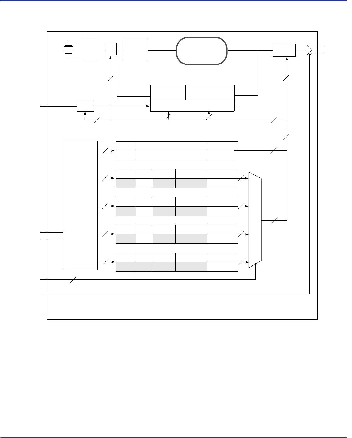
Principles of Operation
The block diagram consists of the internal 3
RD
overtone crystal and
oscillator which provide the reference clock f
XTAL
of either 114.285
MHz or 100 MHz. The PLL includes the FemtoClock NG VCO along
with the Pre-divider (P), the feedback divider (M) and the post divider
(N). The P, M, and N dividers determine the output frequency based
on the f
XTAL
reference and must be configured correctly for proper
operation. The feedback divider is fractional supporting a huge
number of output frequencies. The configuration of the feedback
divider to integer-only values results in an improved output phase
noise characteristics at the expense of the range of output
frequencies. In addition, internal registers are used to hold up to four
different factory pre-set P, M, and N configuration settings. These
default pre-sets are stored in the I
2
C registers at power-up. Each
configuration is selected via the the FSEL[1:0] pins and can be read
back using the SCLK and SDATA pins.
The user may choose to operate the device at an output frequency
different than that set by the factory. After power-up, the user may
write new P, N and M settings into one or more of the four
configuration registers and then use the FSEL[1:0] pins to select the
newly programmed configuration. Note that the I
2
C registers are
volatile and a power supply cycle will reload the pre-set factory
default conditions.
If the user does choose to write a different P, M, and N configuration,
it is recommended to write to a configuration which is not currently
selected by FSEL[1:0] and then change to that configuration after the
I
2
C transaction has completed. Changing the FSEL[1:0] controls
results in an immediate change of the output frequency to the
selected register values. The P, M, and N frequency configurations
support an output frequency range 15.476MHz to 866.67MHz and
975MHz to 1,300MHz.
The devices use the fractional feedback divider with a delta-sigma
modulator for noise shaping and robust frequency synthesis
capability. The relatively high reference frequency minimizes phase
noise generated by frequency multiplication and allows more efficient
shaping of noise by the delta-sigma modulator.
The output frequency is determined by the 2-bit pre-divider (P), the
feedback divider (M) and the 7-bit post divider (N). The feedback
divider (M) consists of both a 7-bit integer portion (MINT) and an
18-bit fractional portion (MFRAC) and provides the means for
high-resolution frequency generation. The output frequency f
OUT
is
calculated by:
The four configuration registers for the P, M (MINT & MFRAC) and N
dividers which are named Pn, MINTn, MFRACn and Nn with n=0 to
3. “n” denominates one of the four possible configurations.
As identified previously, the configurations of P, M (MINT & MFRAC)
and N divider settings are stored the I
2
C register, and the
configuration loaded at power-up is determined by the FSEL[1:0]
pins.
Frequency Configuration
An order code is assigned to each frequency configuration
programmed by the factory (default frequencies). For more
information on the available default frequencies and order codes,
please see the Ordering Information Section in this document. For
available order codes, see the FemtoClock NG Ceramic-Package
XO and VCXO Ordering Product Information document.
For more information and guidelines on programming of the device
for custom frequency configurations, the register description, the pull
range programming and the serial interface description, see the
FemtoClock NG Ceramic 5x7 Module Programming Guide.
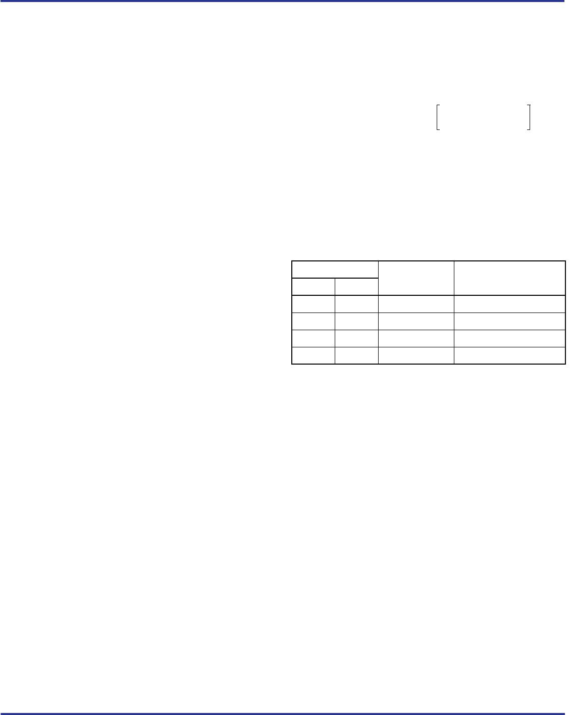
Table 4 Frequency Selection
Input
Selects RegisterFSEL1 FSEL0
0 (def.) 0 (def.) Frequency 0 P0, MINT0, MFRAC0, N0
0 1 Frequency 1 P1, MINT1, MFRAC1, N1
1 0 Frequency 2 P2, MINT2, MFRAC2, N2
1 1 Frequency 3 P3, MINT3, MFRAC3, N3
f
OUT
f
XTAL
1
PN
------------
MINT
MFRAC 0.5+
2
18
-----------------------------------
+=
(1)