IDT8N3QV01 Rev G Data Sheet QUAD-FREQUENCY PROGRAMMABLE-VCXO
IDT8N3QV01GCD REVISION A
MARCH 6, 2012
9 ©2012 Integrated Device Technology, Inc.
Table 6B. AC Characteristics, V
CC
= 3.3V ± 5% or 2.5V ± 5%, V
EE
=
0V, T
A
= -40°C to 85°C
NOTE: Electrical parameters are guaranteed over the specified ambient operating temperature range, which is established when the device
is mounted in a test socket with maintained transverse airflow greater than 500 lfpm. The device will meet specifications after thermal
equilibrium has been reached under these conditions. All AC parameters are characterized with P=1 and pull range = ±250 ppm.
NOTE: XTAL parameters (initial accuracy, temperature stability, aging and total stability) are guaranteed by manufacturing.
NOTE 1: This parameter is defined in accordance with JEDEC standard 65.
NOTE 2: Please refer to the phase noise plots.
NOTE 3: Please see the FemtoClockNG Ceramic 5x7 Modules Programming guide for more information on finding the optimum configuration
for phase noise.
NOTE 4: Integration range: 12kHz-20MHz.
NOTE 5: Integration range: 1kHz-40MHz.
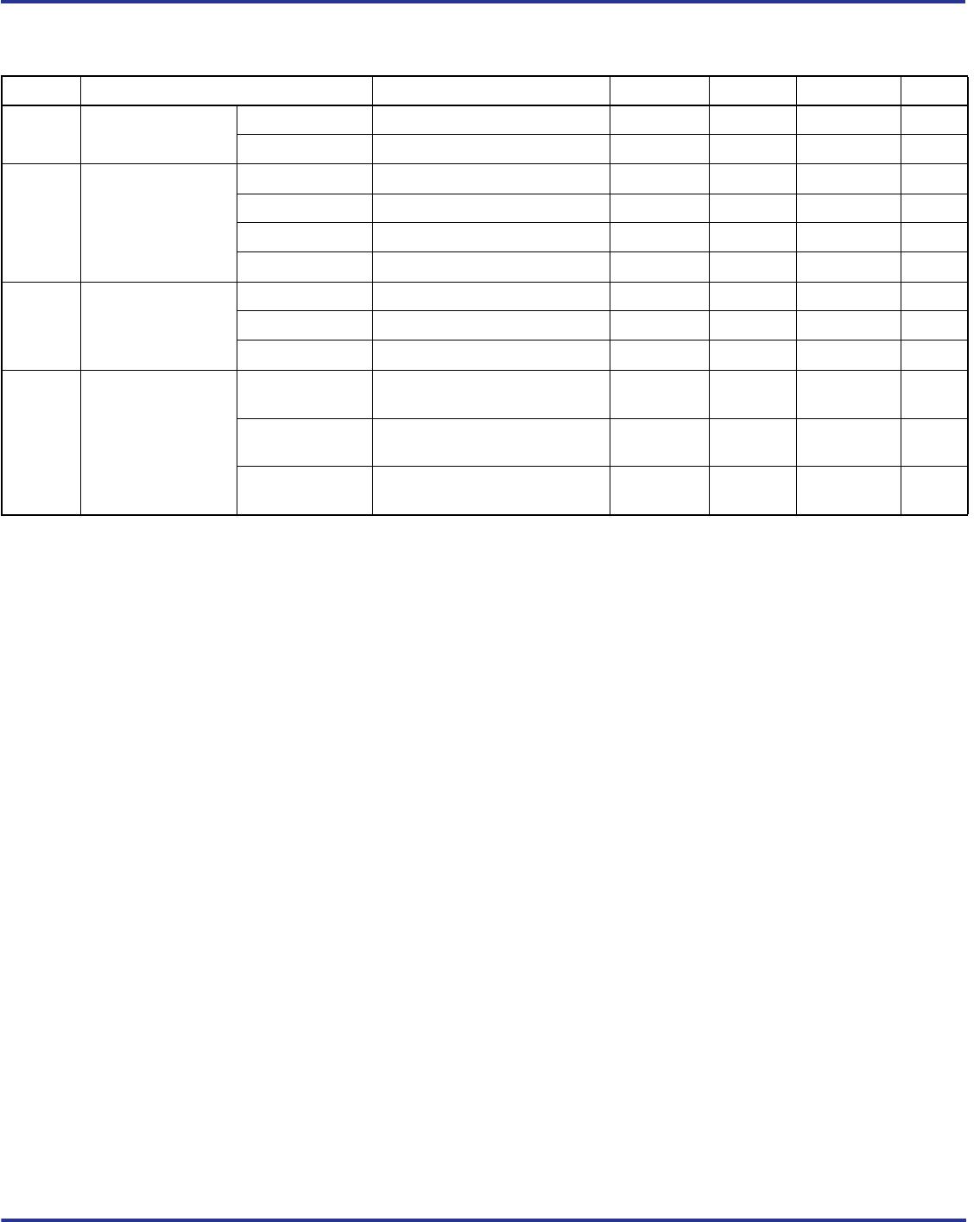
Symbol Parameter Test Conditions Minimum Typical Maximum Units
f
OUT
Output Frequency Q, nQ
Output Divider, N = 3 to126 15.476 866.67 MHz
Output Divider, N = 2 975 1,300 MHz
f
I
Initial Accuracy Measured at 25°C ±10 ppm
f
S
Temperature Stability
Option code = A or B ±100 ppm
Option code = E or F ±50 ppm
Option code = K or L ±20 ppm
f
A
Aging
Frequency drift over 10 year life ±3 ppm
Frequency drift over 15 year life ±5 ppm
f
T
Total Stability
Option code A or B (10 year life) ±113 ppm
Option code E or F (10 year life) ±63 ppm
Option code K or L (10 year life) ±33 ppm
tjit(cc) Cycle-to-Cycle Jitter; NOTE 1 20 ps
tjit(per) RMS Period Jitter; NOTE 1 2.85 4 ps
tjit(Ø)
RMS Phase Jitter (Random)
Fractional PLL feedback and
f
XTAL
=114.285MHz (0xxx order
codes)
17 MHz f
OUT
1300MHz,
NOTE 2,3,4
0.475 0.990 ps
f
OUT
156.25MHz, NOTE 2, 3, 4 0.487 0.757 ps
f
OUT
156.25MHz, NOTE 2, 3, 5 0.614 ps
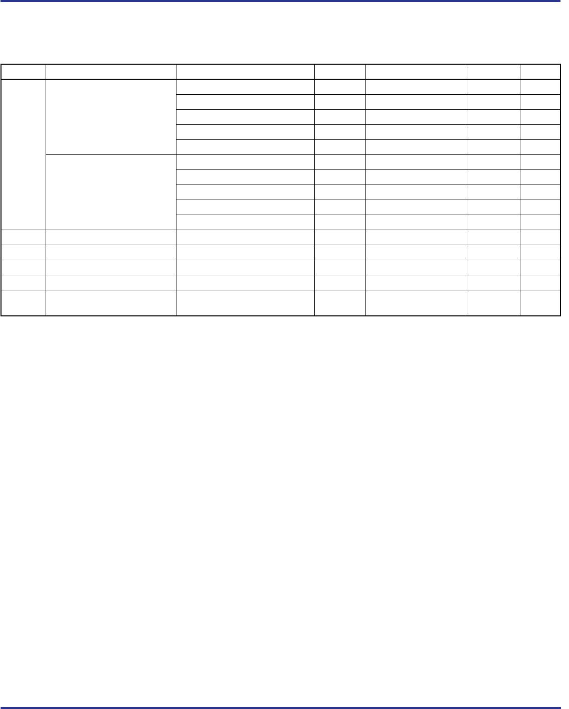
N
(100)
Single-side band phase noise,
100Hz from Carrier
156.25MHz -72.0 dBc/Hz
N
(1k)
Single-side band phase noise,
1kHz from Carrier
156.25MHz -99.0 dBc/Hz
N
(10k)
Single-side band phase noise,
10kHz from Carrier
156.25MHz -125.7 dBc/Hz
N
(100k)
Single-side band phase noise,
100kHz from Carrier
156.25MHz -129.5 dBc/Hz
N
(1M)
Single-side band phase noise,
1MHz from Carrier
156.25MHz -140.5 dBc/Hz
N
(10M)
Single-side band phase noise,
10MHz from Carrier
156.25MHz -144.4 dBc/Hz
PSNR Power Supply Noise Rejection
50 MV Sinusoidal Noise
1kHz - 50 kHz
-54 db
t
R
/ t
F
Output Rise/Fall Time 20% to 80% 100 425 ps
odc Output Duty Cycle 45 55 %
t
OSC
Device startup time after power-up 20 ms
t
SET
Output frequency settling time after
FSEL0 and FSEL1 values are
changed
470 µs