Data Sheet ADF4113HV
Rev. B | Page 9 of 20
CIRCUIT DESCRIPTION
REFERENCE INPUT SECTION
The reference input stage is shown in Figure 14. SW1 and SW2
are normally closed switches (NC in Figure 14). SW3 is normally
open (NO in Figure 14). When power-down is initiated, SW3 is
closed and SW1 and SW2 are opened. This ensures that there is
no loading of the REF
IN
pin on power-down.
BUFFER
TO R COUNTER
REF
IN
100k
NC
SW2
SW3
NO
NC
SW1
POWER-DOWN
CONTROL
06223-014
Figure 14. Reference Input Stage
RF INPUT STAGE
The RF input stage is shown in Figure 15. It is followed by a
two-stage limiting amplifier to generate the current-mode logic
(CML) clock levels needed for the prescaler.
AV
DD
AGND
500
500
1.6V
BIAS
GENERATOR
RF
IN
A
RF
IN
B
06223-015
Figure 15. RF Input Stage
PRESCALER (P/P + 1)
Together with the A and B counters, the dual-modulus prescaler
(P/P + 1) enables the large division ratio, N, to be realized by
N = BP + A
The dual-modulus prescaler, operating at CML levels, takes the
clock from the RF input stage and divides it down to a manageable
frequency for the CMOS A and CMOS B counters. The pre-
scaler is programmable; it can be set in software to 8/9, 16/17,
32/33, or 64/65. It is based on a synchronous 4/5 core.
A AND B COUNTERS
The A and B CMOS counters combine with the dual-modulus
prescaler to allow a wide ranging division ratio in the PLL
feedback counter. The counters are specified to work when the
prescaler output is 200 MHz or less (for AV
DD
= 5 V). Thus,
with an RF input frequency of 2.5 GHz, a prescaler value of
16/17 is valid but a value of 8/9 is not.
Pulse Swallow Function
The A and B counters, in conjunction with the dual-modulus
prescaler, make it possible to generate output frequencies that
are spaced only by the reference frequency divided by R. The
equation for the VCO frequency is
f
VCO
= [(P × B) + A]f
REFIN
/R
where:
f
VCO
= output frequency of external voltage controlled
oscillator (VCO).
P = preset modulus of dual-modulus prescaler.
B = preset divide ratio of binary 13-bit counter (3 to 8191).
A = preset divide ratio of binary 6-bit swallow counter (0 to 63).
f
REFIN
= output frequency of the external reference frequency
oscillator.
R = preset divide ratio of binary 14-bit programmable reference
counter (1 to 16,383).
13-BIT B
COUNTER
6-BIT A
COUNTER
PRESCALER
P/P + 1
FROM RF
INPUT STAGE
MODULUS
CONTROL
N=BP+A
LOAD
LOAD
TO PFD
0
6223-016
Figure 16. A and B Counters
R COUNTER
The 14-bit R counter allows the input reference frequency to be
divided down to produce the reference clock to the phase fre-
quency detector (PFD). Division ratios from 1 to 16,383 are
allowed.
ADF4113HV Data Sheet
Rev. B | Page 10 of 20
PHASE FREQUENCY DETECTOR (PFD) AND
CHARGE PUMP
The PFD takes inputs from the R counter and N counter and
produces an output proportional to the phase and frequency
difference between them. Figure 17 is a simplified schematic.
The PFD includes a programmable delay element that controls
the width of the antibacklash pulse. This pulse ensures that
there is no dead zone in the PFD transfer function and mini-
mizes phase noise and reference spurs. Two bits in the reference
counter latch, ABP2 and ABP1, control the width of the pulse.
See Figure 20. The only recommended setting for the antiback-
lash pulse width is 7.2 ns.
PROGRAMMABLE
DELAY
U3
CLR2
Q2
D2
U2
CLR1
Q1
D1
CHARGE
PUMP
DOWN
UP
HIGH
HIGH
U1
ABP1 ABP2
R DIVIDER
N DIVIDER
CP OUTPUT
R DIVIDER
N DIVIDER
CP
CPGND
V
P
06223-017
Figure 17. PFD Simplified Schematic and Timing (in Lock)
MUXOUT AND LOCK DETECT
The output multiplexer on the ADF4113HV allows the user to
access various internal points on the chip. The state of MUXOUT
is controlled by M3, M2, and M1 in the function latch. Figure 22
shows the full truth table (function latch map). Figure 18 shows
the MUXOUT section in block diagram form.
CO
NT
R
OL
MUX
DV
D
D
MUXOU
T
DGND
ANA
L
OG L
OCK
DETECT
D
IGI
T
A
L
L
O
CK
DE
TE
C
T
R
CO
UN
T
E
R
O
U
T
P
U
T
N
CO
UN
TE
R O
U
TP
U
T
S
DO
UT
06223-018
Figure 18. MUXOUT Circuit
Lock Detect
MUXOUT can be programmed for two types of lock detect:
digital lock detect and analog lock detect.
Digital lock detect is active high. When LDP in the AB counter
latch is set to 0, digital lock detect is set high when the phase
error on five consecutive phase detector (PD) cycles is less than
10 ns. With LDP set to 1, five consecutive cycles of less than
3 ns are required to set the lock detect. It stays high until a phase
error greater than 25 ns is detected on any subsequent PD cycle.
Operate the N-channel, open-drain, analog lock detect with a
10 kΩ nominal external pull-up resistor. When lock has been
detected, this output is high with narrow low-going pulses.
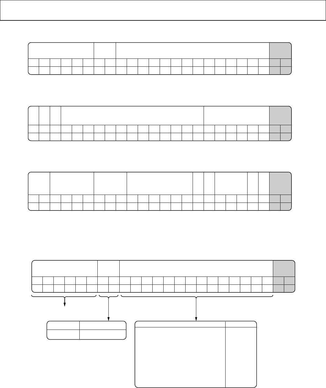
INPUT SHIFT REGISTER
The ADF4113HV digital section includes a 24-bit input shift
register, a 14-bit R counter, and a 19-bit N counter comprising
a 6-bit A counter and a 13-bit B counter. Data is clocked into
the 24-bit shift register on each rising edge of CLK, MSB first.
Data is transferred from the shift register to one of three latches
on the rising edge of LE. The destination latch is determined by
the state of the two control bits (C2, C1) in the shift register.
These are the two LSBs, DB1 and DB0, as shown in Figure 2.
The truth table for these bits is shown in Table 6. Figure 19
shows a summary of how the latches are programmed.
Table 6. C2, C1 Truth Table
Control Bits
C2 C1 Data Latch
0 0 R counter
0 1 N counter (A and B)
1 0 Function latch (including prescaler)
Data Sheet ADF4113HV
Rev. B | Page 11 of 20
Latch Summary
DB23 DB22
DB21 DB20
DB19
DB18
DB17
DB16
DB15
DB14
DB13
DB12
DB11 DB10 DB9 DB8 DB7 DB6 DB5 DB4 DB3
DB2 DB1
DB0
0
0
0 0 0 0 ABP2 ABP1 R14 R13 R12
R11
R10
R9 R8
R7
R6
R5
R4
R3
R2
R1
C2(0) C1(0)
RESERVED
14-BIT REFERENCE COUNTER
CONTROL
BITS
REFERENCE COUNTER LATCH
DB23
DB22 DB21 DB20 DB19 DB18 DB17 DB16 DB15 DB14 DB13 DB12 DB11
DB10
DB9 DB8
DB7
DB6
DB5
DB4
DB3
DB2 DB1 DB0
0 L1 0 B13
B12
B11 B10
B9
B8
B7
B6
B5
B4 B3 B2 B1 A6 A5 A4 A3 A2 A1
C2(0) C1(1)
CONTROL
BITS
RE-
SERVED
LD
PREC
RE-
SERVED
13-BIT B COUNTER
6-BIT A COUNTER
N COUNTER LATCH
DB23 DB22
DB21 DB20
DB19 DB18 DB17 DB16
DB15 DB14 DB13
DB12 DB11
DB10
DB9 DB8 DB7 DB6
DB5 DB4 DB3
DB2
DB1 DB0
P2 P1
0
0 0
0 CP3 CP2 CP1 0 0
0
0 0
0 F4 F3 M3 M2
M1 F2
F1 C2(1)
C1(0)
CONTROL
BITS
CP THREE-
STATE
PD
POLARITY
PRE-
SCALER
VALUE
RESERVED
CURRENT
SETTING RESERVED
MUXOUT
CONTROL
POWER
DOWN
COUNTER
RESET
FUNCTION LATCH
06223-019
ANTI-
BACKLASH
PULSE
WIDTH
Figure 19. Latch Summary Tables
Reference Counter Latch Map
DB23 DB22 DB21 DB20 DB19
DB18 DB17 DB16 DB15 DB14 DB13 DB12 DB11 DB10
DB9 DB8 DB7
DB6 DB5 DB4
DB3 DB2
DB1 DB0
0
0 0 0 0
0 ABP2 ABP1
R14 R13
R12 R11 R10
R9 R8 R7 R6 R5 R4 R3 R2
R1 C2(0) C1(0)
RESERVED
ANTI-
BACKLASH
PULSE
WIDTH
14-BIT REFERENCE COUNTER
CONTROL
BITS
THESE BITS MUST BE SET AS
INDICATED FOR NORMAL OPERATION
R14 R13 R12 .......... R3 R2 R1
DIVIDE RATIO
0 0 0 .......... 0 0 1
1
0 0 0 .......... 0 1 0 2
0 0 0 .......... 0 1 1
3
0 0
0 .......... 1 0 0 4
. . . .......... . . . .
. . . .......... . . . .
.
. . .......... . . . .
1 1 1 .......... 1 0 0
16380
1 1 1 .......... 1 0 1
16381
1 1 1 .......... 1
1 0 16382
1 1 1 .......... 1
1 1 16383
06223-020
ABP2 ABP1
ANTI-BACKLASH
PULSE WIDTH
1 0 7.2ns (ONLY ALLOWED
SETTING)
Figure 20. Reference Counter Latch Bit Map

ADF4113HVBRUZ-RL7

Mfr. #:
Manufacturer:
Analog Devices Inc.
Description:
Phase Locked Loops - PLL High VTG Charge Pump
Lifecycle:
New from this manufacturer.
Delivery:
DHL FedEx Ups TNT EMS
Payment:
T/T Paypal Visa MoneyGram Western Union