Data Sheet ADF4113HV
Rev. B | Page 15 of 20
APPLICATIONS
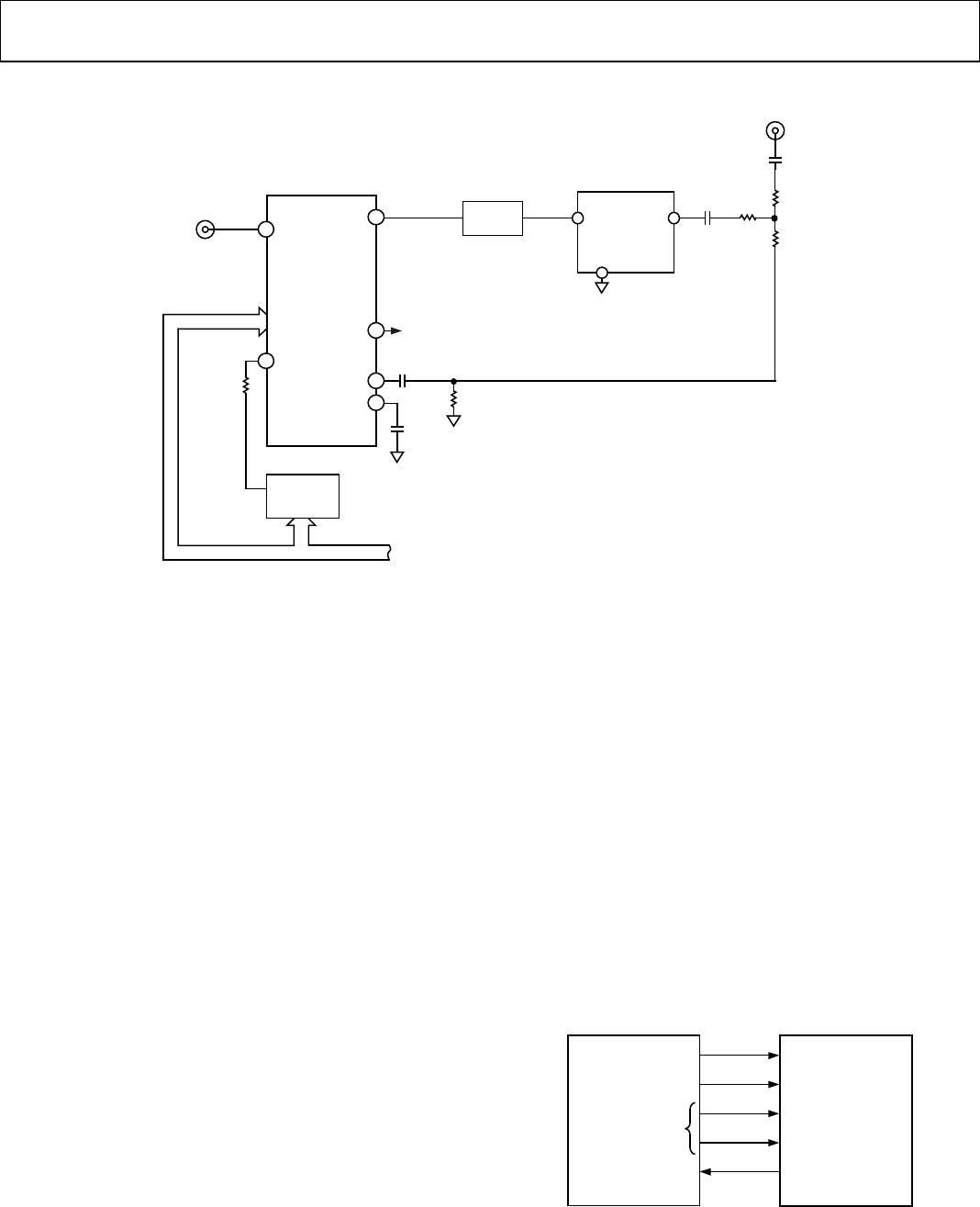
ADF4113HV
2.7kΩ
VCO
GND
18Ω
100pF
100pF
18Ω
18Ω
RF
OUT
FREF
IN
51Ω
100pF
100pF
RF
IN
A
RF
IN
B
R
SET
REF
IN
CP
CE
CLK
DATA
LE
SPI-COMPATIBLE SERIAL BUS
MUXOUT
LOCK
DETECT
INPUT OUTPUT
2
14
6
5
1
8
LOOP
FILTER
NOTES
1. POWER SUPPLY CONNECTIONS AND DECOUPLING
CAPACITORS ARE OMITTED FOR CLARITY.
AD5320
12-BIT
V-OUT DAC
06223-023
Figure 23. Driving the R
SET
Pin with a Digital-to-Analog Converter
USING A DIGITIAL-TO-ANALOG CONVERTER TO
DRIVE THE R
SET
PIN
A digital-to-analog converter (DAC) can be used to drive the
R
SET
pin of the ADF4113HV, thus increasing the level of control
over the charge pump current (I
CP
). This can be advantageous in
wideband applications where the sensitivity of the VCO varies
over the tuning range. To compensate for this, I
CP
can be varied
to maintain good phase margin and ensure loop stability. See
Figure 23 for this configuration.
INTERFACING
The ADF4113HV has a simple SPI®-compatible serial interface
for writing to the device. CLK, DATA, and LE control the data
transfer. When latch enable (LE) goes high, the 24 bits that have
been clocked into the input register on each rising edge of CLK
are transferred to the appropriate latch. See Figure 2 for the
timing diagram and Table 6 for the latch truth table.
The maximum allowable serial clock rate is 20 MHz. This
means that the maximum update rate possible for the device
is 833 kHz, or one update every 1.2 µs. This rate is more than
adequate for systems that have typical lock times in the
hundreds of microseconds.
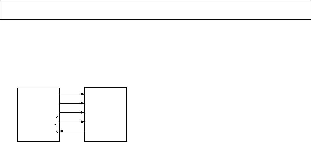
ADuC812 Interface
Figure 24 shows the interface between the ADF4113HV and the
ADuC812 MicroConverter®. Because the ADuC812 is based on
an 8051 core, this interface can be used with any 8051-based
microcontroller. The MicroConverter is set up for SPI master
mode with CPHA = 0. To initiate the operation, the I/O port
driving LE is brought low. Each latch of the ADF4113HV needs
a 24-bit word. This is accomplished by writing three 8-bit bytes
from the MicroConverter to the device. When the third byte
has been written, the LE input should be brought high to
complete the transfer.
I/O port lines on the ADuC812 are also used to control power-
down (CE input), and to detect lock (MUXOUT configured as
lock detect and polled by the port input).
When the ADuC812 is operating in the SPI master mode, the
maximum SCLOCK rate of the ADuC812 is 4 MHz. This
means that the maximum rate at which the output frequency
can be changed is 166 kHz.
SCLOCK
MOSI
I/O PORTS
ADuC812
CLK
DATA
LE
CE
MUXOUT
(LOCK DETECT)
ADF4113HV
06223-024
Figure 24. ADuC812 to ADF4113HV Interface