NB3H63143G
www.onsemi.com
18
APPLICATION GUIDELINES
Crystal Input Interface
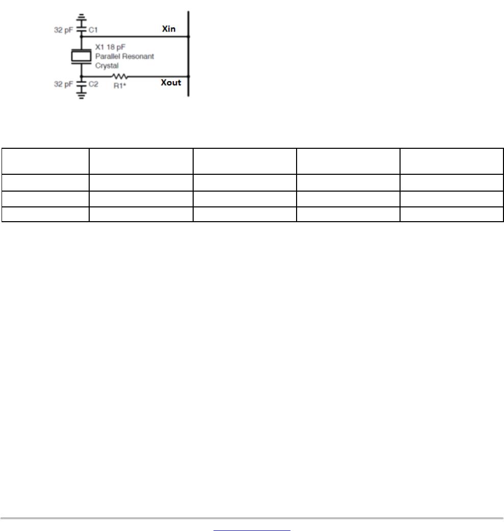
Figure 16 shows the NB3H63143G device crystal
oscillator interface using a typical parallel resonant
fundamental mode crystal. A parallel crystal with loading
capacitance CL = 18 pF would use C1 = 32 pF and C2 =
32 pF as nominal values, assuming 4 pF of stray capacitance
per line.
C
L
+
(
C1 ) Cstray
)
ń2; C1 + C2
The frequency accuracy and duty cycle skew can be
fine−tuned by adjusting the C1 and C2 values. For example,
increasing the C1 and C2 values will reduce the operational
frequency. Note R1 is optional and may be 0 W.
Figure 16. Crystal Interface Loading
Output Interface and Terminations
The NB3H63143G consists of a unique Multi Standard
Output Driver to support LVCMOS/LVTTL, LVPECL,
LVDS, HCSL and CML standards. Termination techniques
required for each of these standards are different to ensure
proper functionality. From the device it is possible to switch
off one output driver and turn on another output driver using
the SEL[1:0] pins as part of the Configuration Settings. The
required termination changes must be considered and taken
care of by the system designer.
LVCMOS/LVTTL Interface
LVCMOS/LVTTL output swings rail−to−rail up to
VDDO supply (minimum 1.8 V) and can drive up to 15 pF
load at higher drive stengths. The output buffer’s drive is
programmable up to four steps, though the drive current will
depend on the step setting as well as the VDDO supply
voltage. (See Figure 17 and Table 8). Drive strength must be
configured high for driving higher loads. The slew rate of the
clock signal increases with higher output current drive for
the same load. The software lets the user choose the load
drive current value per LVCMOS/LVTTL output based on
the VDDO supply selected.
Table 8. LVCMOS/LVTTL DRIVE LEVEL SETTINGS
VDDO Supply
Load Current Setting 3
Max Load Current
Load Current Setting 2 Load Current Setting 1
Load Current Setting 0
Min Load Current
3.3 V 16 mA 12 mA 8 mA 4 mA
2.5 V 12 mA 8 mA 4 mA 2 mA
1.8 V 8 mA 4 mA 2 mA 1 mA
The IDDO current consists of the static current
component (varies with drive) and dynamic current
component. For any VDDO, the IDDO dynamic current
range per LVCMOS output can be approximated by the
following:
IDDO + f
out
*C
load
* VDDO
C
load
includes the load capacitor connected to the output,
the pin capacitor posed by the output pin (typically 5 pF) and
the cap load posed by the receiver input pin. C
load
= (CL +
C
pin
+ C
in
)
An optional series resistor Rs can be connected at the
output for impedance matching, to limit the overshoots and
ringings.