NB3H63143G
www.onsemi.com
5
Clock Input
Input Frequency
The clock input block can be programmed to use
a fundamental mode crystal from 3 MHz to 50 MHz or
a single ended reference clock source from 3 MHz to
200 MHz. When using output frequency modulation for
EMI reduction, for optimal performance, it is recommended
to use crystals with a frequency greater than 6.75 MHz as
input. Crystals with ESR values of up to 150 W are
supported. While using a crystal as input, it is important to
set crystal load capacitor values correctly to achieve good
performance.
Programmable Crystal Load Capacitors
The provision of internal programmable crystal load
capacitors eliminates the necessity of external load
capacitors for standard crystals. The internal load capacitors
can be programmed to any value between 4.36 pF and
20.39 pF with a step size of 0.05 pF. Refer to Table 5 for
recommended maximum load capacitor values for stable
operation. There are three modes of loading the crystal −
with internal chip capacitors only, with external capacitors
only or with the both internal and external capacitors. Check
with the crystal vendor’s load capacitance specification for
setting of the internal load capacitors. The minimum value
of 4.36 pF internal load capacitor need to be considered
while selecting external capacitor value. The internal load
capacitors will be bypassed when using an external
reference clock.
Automatic Gain Control (AGC)
The Automatic Gain Control (AGC) feature adjusts the
gain to the input clock based on its signal strength to
maintain a good quality input clock signal level. This feature
takes care of low clock swings fed from external reference
clocks and ensures proper device operation. It also enables
maximum compatibility with crystals from different
manufacturers, processes, quality and performance. AGC
also takes care of power dissipation in the crystal; avoids
overdriving the crystal and thus extending the crystal life. In
order to calculate the AGC gain accurately and avoid
increasing the jitter on the output clocks, the user needs to
provide the crystal load capacitance as well as other crystal
parameters like ESR and shunt capacitance (C0).
Programmable Clock Outputs
Output Type and Frequency
The NB3H63143G provides three independent single
ended LVCMOS/LVTTL outputs, or one single ended
LVCMOS/LVTTL output and one LVPECL/LVDS/HCSL/
CML differential output. The device supports any single
ended output or differential output frequency from 8 kHz up
to 200 MHz with or without frequency modulation. All
outputs have individual output enable pins (refer to the
Output Enable/Disable section on page 7). It should be
noted that certain combinations of output frequencies and
spread spectrum configurations may not be recommended
for optimal and stable operation.
For differential clocking, CLK0 and CLK1 can be
configured as LVPECL, LVDS, HCSL or CML. While using
differential signaling format at the output, it is required to
use only VDDO1 as output supply and use only the OE1 pin
for the output enable function. (refer to the Application
Schematic in Figure 4). When all 3 outputs are single ended,
VDDO0 and OE0 have normal functionality.
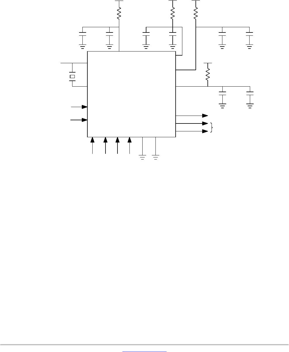
Figure 4. Application Setup for Differential Output Configuration
Crystal or
Reference
Clock Input
NB3H63143G
PD#
OE2
OE1
OE0
LVPECL/LVDS/HCSL/CML
Single Ended Clock
Differential Clock
XIN/CLKIN
XOUT
VDDO2
VDDO1
VDDO0
CLK1
CLK0
CLK2
VDDO1 ≤ VDD
VDDO2 ≤ VDD
Programmable Output Drive
The drive strength or output current of each of the
LVCMOS clock outputs is programmable independently.
For each VDDO supply voltage, four distinct levels of
LVCMOS output drive strengths can be selected as
mentioned in DC Electrical Characteristics. This feature
provides further load drive and signal conditioning as per the
application requirement.
PLL BYPASS Mode
PLL Bypass mode can be used to buffer the input clock on
any of the outputs or all of the outputs. Any of the clock
outputs can be programmed to generate a copy of the input
clock.