NB3H63143G
www.onsemi.com
22
amplitude of the overshoots and subsequent ripples. The
ripple frequency is dependant on the signal travel time from
the receiver to the source. Shorter traces results in higher
ripple frequency, as the trace gets longer the travel time
increases, reducing the ripple frequency. The ripple
frequency is independent of signal frequency, and only
depends on the trace length and the propogation delay. For
eg. On an FR4 PCB with approximately 150 ps/inch of
propogation rate on a 2 inch trace, the ripple frequency = 1
/ (150 ps * 2 inch * 5) = 666.6 MHz; [5 = number of times
the signal travels, 1 trip to receiver plus 2 additional round
trips].
PCB traces should be terminated when trace length >= tr/f
/ (2* tprate); tf/t = rise/ fall time of signal, tprate =
propagation rate of trace.
Ringing
Overshoot
(Positive)
Overshoot
(Negative)
Figure 24. Signal Reflection Components
PCB Design Recommendation
For a clean clock signal waveform it is necessary to have
a clean power supply for the device. The device must be
isolated from system power supply noise. A 0.1 mF and a
2.2 mF decoupling capacitor should be mounted on the
component side of the board as close to the VDD pin as
possible. No vias should be used between the decoupling
capacitor and VDD pin. The PCB trace to VDD pin and the
ground via should be kept as thick and as short as possible.
All the VDD pins should have decoupling capacitors.
Stacked power and ground planes on the PCB should be
large. Signal traces should be on the top layer with minimum
vias and discontinuities and should not cross the reference
planes. The termination components must be placed near the
source or the receiver. In an optimum layout all components
are on the same side of the board, minimizing vias through
other signal layers.
Device Applications
The NB3H63143G is targeted mainly for the Consumer
market segment and can be used as per the examples below.
Clock Generator
Consumer applications like a Set top Box, have multiple
sub−systems and standard interfaces and require multiple
reference clock sources at various locations in the system.
This part can function as a clock generating IC for such
applications generating a reference clock for interfaces like
USB, Ethernet, Audio/Video, ADSL, PCI etc.
Figure 25. Application as Clock Generator
Phase
Detector
Charge
Pump
VCO
CMOS/
DIFF
buffer
CMOS /
DIFF
buffer
CMOS
buffer
Feedback
Divider
XIN/CLKIN
XOUT
Crystal
CLK0
VDD
GND
Reference
Clock
Output
Divider
Output
Divider
Output
Divider
PLL Block
VDDO0
CLK1
VDDO1
CLK2
VDDO2
PLL Bypass Mode
Clock Buffer/
Crystal
Oscillator And
AGC
SEL1SEL0
Configuration
Memory
Frequency
and SS
Output control
PD#
Input
Decoder
Crystal /Clock Control
OE0
OE1
OE2
GNDO
25MHz
27MHz
48MHz
25MHz
Video
USB
Ethernet
Buffer and Logic/Level Translator
The NB3H63143G is useful as a simple CMOS Buffer in
PLL bypass mode. One or more outputs can use the PLL
Bypass mode to generate the buffered outputs. If the PLL is
configured to use spread spectrum, all outputs using PLL
Bypass feature will not be subjected to the spread spectrum.
The device can be simultaneously used as logic translator for
converting the LVCMOS input clock to LVPECL, LVDS,
HCSL, CML, or LVCMOS (with different output voltage
level).
For instance in applications like an LCD monitor, for
converting the LVCMOS input clock to LVDS output.
NB3H63143G
www.onsemi.com
23
NOTE: Since the device requirement is VDDO VDD, LVCMOS signal level cannot be translated to a higher level of LVCMOS voltage.
Figure 26. Application as Level Translator
Phase
Detector
Charge
Pump
VCO
CMOS/
DIFF
buffer
CMOS /
DIFF
buffer
CMOS
buffer
Feedback
Divider
XIN/CLKIN
XOUT
CLK0
VDD
GND
Reference
Clock
Output
Divider
Output
Divider
Output
Divider
PLL Block
VDDO0
CLK1
VDDO1
CLK2
VDDO2
PLL Bypass Mode
Clock Buffer/
Crystal
Oscillator And
AGC
SEL1SEL0
Configuration
Memory
Frequency
and SS
Output control
PD#
Input
Decoder
Crystal /Clock Control
OE0
OE1
OE2
GNDO
LVCMOS
LVDS
LVCMOS
EMI Attenuator
Spread spectrum through frequency modulation
technique enables the reduction of EMI radiated from the
high frequency clock signals by spreading the spectral
energy to the nearby frequencies. While using frequency
modulation, the same selection is applied to all the PLL
clock outputs (not bypass outputs) even if they are at
different frequencies. In Figure 27, CLK0 uses the PLL and
hence is subjected to the spread spectrum modulation while
CLK1 and CLK2 use the PLL Bypass mode and hence are
not subjected to the spread spectrum modulation.
Figure 27. Application as EMI Attenuator
Phase
Detector
Charge
Pump
VCO
CMOS/
DIFF
buffer
CMOS /
DIFF
buffer
CMOS
buffer
Feedback
Divider
XIN/CLKIN
XOUT
Crystal
CLK0
VDD
GND
Reference
Clock
Output
Divider
Output
Divider
Output
Divider
PLL Block
VDDO0
CLK1
VDDO1
CLK2
VDDO2
PLL Bypass Mode
Clock Buffer/
Crystal
Oscillator And
AGC
SEL1SEL0
Configuration
Memory
Frequency
and SS
Output control
PD#
Input
Decoder
Crystal /Clock Control
OE0
OE1
OE2
GNDO
12MHz
12MHz +/- 0.375 %
12MHz
12MHz
CPU
USB1
USB2
ORDERING INFORMATION
Device Case Package Type Shipping
NB3H63143G00MNR2G 485AE QFN−16
(Pb−Free)
Blank Device 3000 / Tape & Reel
NB3H63143GxxMNR2G 485AE QFN−16
(Pb−Free)
Factory Pre−programmed
Device
3000 / Tape & Reel
For information on tape and reel specifications, including part orientation and tape sizes, please refer to our Tape and Reel Packaging
Specifications Brochure, BRD8011/D.
Note: Please contact your ON Semiconductor sales representative for availability in tube.
NB3H63143G
www.onsemi.com
24
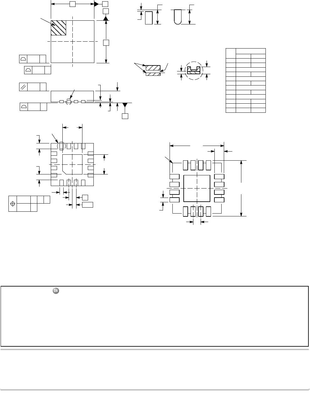
PACKAGE DIMENSIONS
QFN16 3x3, 0.5P
CASE 485AE
ISSUE B
16X
SEATING
PLANE
L
D
E
0.15 C
A
A1
e
D2
E2
b
1
4
58
12
9
16 13
NOTES:
1. DIMENSIONING AND TOLERANCING PER
ASME Y14.5M, 1994.
2. CONTROLLING DIMENSION: MILLIMETERS.
3. DIMENSION b APPLIES TO PLATED
TERMINAL AND IS MEASURED BETWEEN
0.25 AND 0.30 MM FROM TERMINAL.
4. COPLANARITY APPLIES TO THE EXPOSED
PAD AS WELL AS THE TERMINALS.
5. OUTLINE MEETS JEDEC DIMENSIONS PER
MO−220, VARIATION VEED−6.
B
A
0.15
C
TOP VIEW
SIDE VIEW
BOTTOM VIEW
PIN 1
LOCATION
0.10 C
0.08 C
(A3)
C
16X
0.10 C
0.05
C
A B
NOTE 3
K
16X
L1
DETAIL A
L
ALTERNATE TERMINAL
CONSTRUCTIONS
A1
A3
L
DETAIL B
MOLD CMPDEXPOSED Cu
ALTERNATE
CONSTRUCTIONS
DETAIL B
DETAIL A
*For additional information on our Pb−Free strategy and soldering
details, please download the ON Semiconductor Soldering and
Mounting Techniques Reference Manual, SOLDERRM/D.
SOLDERING FOOTPRINT*
0.50
PITCH
3.30
DIMENSIONS: MILLIMETERS
0.65
16X
0.30
16X
OUTLINE
PACKAGE
RECOMMENDED
1
3.30
DIM MIN MAX
MILLIMETERS
A 0.80 1.00
A1 0.00 0.05
b 0.18 0.30
D 3.00 BSC
D2 1.25 1.55
E 3.00 BSC
E2 1.25 1.55
e 0.50 BSC
L 0.30 0.50
A3 0.20 REF
L1 0.00 0.15
K
NOTE 4
e/2
0.20 −−
ON Semiconductor and the are registered trademarks of Semiconductor Components Industries, LLC (SCILLC) or its subsidiaries in the United States and/or other countries.
SCILLC owns the rights to a number of patents, trademarks, copyrights, trade secrets, and other intellectual property. A listing of SCILLC’s product/patent coverage may be accessed
at www.onsemi.com/site/pdf/Patent−Marking.pdf. SCILLC reserves the right to make changes without further notice to any products herein. SCILLC makes no warranty, representation
or guarantee regarding the suitability of its products for any particular purpose, nor does SCILLC assume any liability arising out of the application or use of any product or circuit, and
specifically disclaims any and all liability, including without limitation special, consequential or incidental damages. “Typical” parameters which may be provided in SCILLC data sheets
and/or specifications can and do vary in different applications and actual performance may vary over time. All operating parameters, including “Typicals” must be validated for each
customer application by customer’s technical experts. SCILLC does not convey any license under its patent rights nor the rights of others. SCILLC products are not designed, intended,
or authorized for use as components in systems intended for surgical implant into the body, or other applications intended to support or sustain life, or for any other application in which
the failure of the SCILLC product could create a situation where personal injury or death may occur. Should Buyer purchase or use SCILLC products for any such unintended or
unauthorized application, Buyer shall indemnify and hold SCILLC and its officers, employees, subsidiaries, affiliates, and distributors harmless against all claims, costs, damages, and
expenses, and reasonable attorney fees arising out of, directly or indirectly, any claim of personal injury or death associated with such unintended or unauthorized use, even if such claim
alleges that SCILLC was negligent regarding the design or manufacture of the part. SCILLC is an Equal Opportunity/Affirmative Action Employer. This literature is subject to all applicable
copyright laws and is not for resale in any manner.
P
UBLICATION ORDERING INFORMATION
N. American Technical Support: 800−282−9855 Toll Free
USA/Canada
Europe, Middle East and Africa Technical Support:
Phone: 421 33 790 2910
Japan Customer Focus Center
Phone: 81−3−5817−1050
NB3H63143G/D
LITERATURE FULFILLMENT:
Literature Distribution Center for ON Semiconductor
19521 E. 32nd Pkwy, Aurora, Colorado 80011 USA
Phone: 303−675−2175 or 800−344−3860 Toll Free USA/Canada
Fax: 303−675−2176 or 800−344−3867 Toll Free USA/Canada
Email: orderlit@onsemi.com
ON Semiconductor Website: www.onsemi.com
Order Literature: http://www.onsemi.com/orderlit
For additional information, please contact your loc
al
Sales Representative

NB3H63143G00MNR2G

Mfr. #:
Manufacturer:
ON Semiconductor
Description:
Clock Generators & Support Products PROGRAMMABLE CLOCK G
Lifecycle:
New from this manufacturer.
Delivery:
DHL FedEx Ups TNT EMS
Payment:
T/T Paypal Visa MoneyGram Western Union

Products related to this Datasheet