NOVEMBER 1997 - REVISED JANUARY 2007
Specifications are subject to change without notice.
Customers should verify actual device performance in their specific applications.
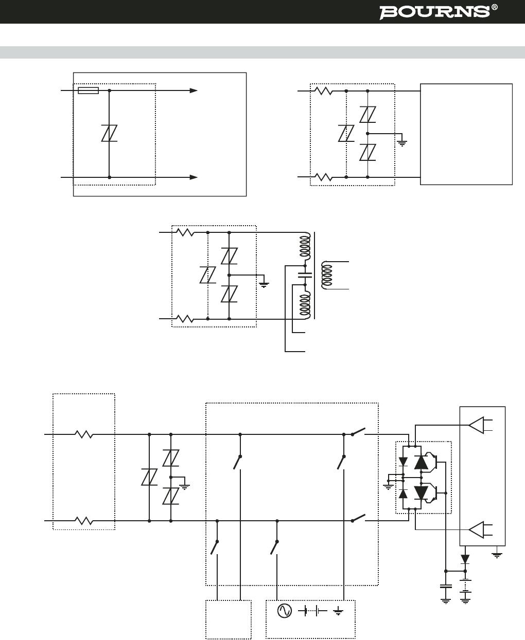
The protector can withstand currents applied for times not exceeding those shown in Figure 8. Currents that exceed these times must be
terminated or reduced to avoid protector failure. Fuses, PTC (Positive Temperature Coefficient) resistors and fusible resistors are overcurrent
protection devices which can be used to reduce the current flow. Protective fuses may range from a few hundred milliamperes to one ampere.
In some cases, it may be necessary to add some extra series resistance to prevent the fuse opening during impulse testing. The current versus
time characteristic of the overcurrent protector must be below the line shown in Figure 8. In some cases, there may be a further time limit
imposed by the test standard (e.g. UL 1459 wiring simulator failure).
AC Power Testing
Capacitance
APPLICATIONS INFORMATION
Normal System Voltage Levels
TISP4xxxH3BJ Overvoltage Protector Series
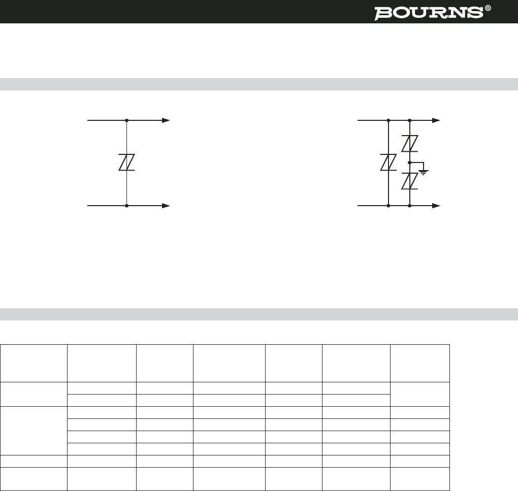
The protector characteristic off-state capacitance values are given for d.c. bias voltage, V
D
, values of 0, -1 V, -2 V and -50 V. Where possible,
values are also given for -100 V. Values for other voltages may be calculated by multiplying the V
D
= 0 capacitance value by the factor given in
Figure 6. Up to 10 MHz, the capacitance is essentially independent of frequency. Above 10 MHz, the effective capacitance is strongly
dependent on connection inductance. In many applications, such as Figure 15 and Figure 17, the typical conductor bias voltages will be about
-2 V and -50 V. Figure 7 shows the differential (line unbalance) capacitance caused by biasing one protector at -2 V and the other at -50 V.
The protector should not clip or limit the voltages that occur in normal system operation. For unusual conditions, such as ringing without the
line connected, some degree of clipping is permissible. Under this condition, about 10 V of clipping is normally possible without activating the
ring trip circuit.
Figure 10 allows the calculation of the protector V
DRM
value at temperatures below 25 °C. The calculated value should not be less than the
maximum normal system voltages. The TISP4265H3BJ, with a V
DRM
of 200 V, can be used for the protection of ring generators producing
100 V r.m.s. of ring on a battery voltage of -58 V (Th2 and Th3 in Figure 17). The peak ring voltage will be 58 + 1.414*100 = 199.4 V. However,
this is the open circuit voltage and the connection of the line, and its equipment will reduce the peak voltage. In the extreme case of an
unconnected line, clipping the peak voltage to 190 V should not activate the ring trip. This level of clipping would occur at the temperature
when the V
DRM
has reduced to 190/200 = 0.95 of its 25 °C value. Figure 10 shows that this condition will occur at an ambient temperature of
-22 °C. In this example, the TISP4265H3BJ will allow normal equipment operation provided that the minimum expected ambient temperature
does not fall below -22 °C.
JESD51 Thermal Measurement Method
To standardize thermal measurements, the EIA (Electronic Industries Alliance) has created the JESD51 standard. Part 2 of the standard
(JESD51-2, 1995) describes the test environment. This is a 0.0283 m
3
(1 ft
3
) cube which contains the test PCB (Printed Circuit Board)
horizontally mounted at the center. Part 3 of the standard (JESD51-3, 1996) defines two test PCBs for surface mount components; one for
packages smaller than 27 mm (1.06 ’’) on a side and the other for packages up to 48 mm (1.89 ’’). The SMBJ measurements used the smaller
76.2 mm x 114.3 mm (3.0 ’’ x 4.5 ’’) PCB. The JESD51-3 PCBs are designed to have low effective thermal conductivity (high thermal resis-
tance) and represent a worse case condition. The PCBs used in the majority of applications will achieve lower values of thermal resistance and
so can dissipate higher power levels than indicated by the JESD51 values.