IDT72V805/72V815/72V825/72V835/72V845
3.3 V CMOS DUAL SyncFIFO™ 256 x 18, 512 x 18, 1,024 x 18, 4,096 x 18
COMMERCIAL AND INDUSTRIAL
TEMPERATURE RANGES
3
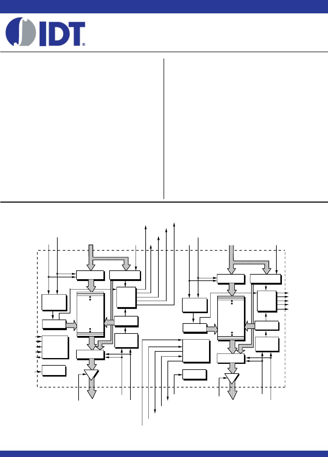
PIN DESCRIPTION
Symbol Name I/O Description
DA
0–DA17 Data Inputs I Data inputs for an 18-bit bus.
DB0-DB17
RSA Reset I When RS is set LOW, internal read and write pointers are set to the first location of the RAM array, FF and
RSB PAF go HIGH, and PAE and EF go LOW. A reset is required before an initial WRITE after power-up.
WCLKA Write Clock I When WEN is LOW, data is written into the FIFO on a LOW-to-HIGH transition of WCLK, if the FIFO is not full.
WCLKB
WENA Write Enable I When WEN is LOW, data is written into the FIFO on every LOW-to-HIGH transition of WCLK.
WENB When WEN is HIGH, the FIFO holds the previous data. Data will not be written into the FIFO if the FF is LOW.
RCLKA Read Clock I When REN is LOW, data is read from the FIFO on a LOW-to-HIGH transition of RCLK, if the FIFO is not
RCLKB empty.
RENA Read Enable I When REN is LOW, data is read from the FIFO on every LOW-to-HIGH transition of RCLK. When REN
RENB is HIGH, the output register holds the previous data. Data will not be read from the FIFO if the EF is low.
OEA Output Enable I When OE is LOW, the data output bus is active. If OE is HIGH, the output data bus will be in a
OEB high-impedance state.
LDA Load I When LD is LOW, data on the inputs D0–D11 is written to the offset and depth registers on the LOW-to-HIGH
LDB transition of the WCLK, when WEN is LOW. When LD is LOW, data on the outputs Q0–Q11 is read from the
offset and depth registers on the LOW-to-HIGH transition of the RCLK, when REN is LOW.
FLA First Load I In the single device or width expansion configuration, FL together with WXI and RXI etermine if the mode is IDT
FLB Standard mode or First Word Fall Through (FWFT) mode, as well as whether the PAE/PAF flags are synchronous
or asynchronous. (See Table I.) In the Daisy Chain Depth Expansion configuration, FL is grounded on the first
device (first load device) and set to HIGH for all other devices in the Daisy Chain.
WXIA Write Expansion I In the single device or width expansion configuration, WXI together with FL and RXI Input determine if the mode
WXIB is IDT Standard mode or FWFT mode, as well as whether the PAE/PAF flags are synchronous or asynchronous.
(See Table 1.) In the Daisy Chain Depth Expansion configuration, WXI is connected to WXO (Write Expansion
Out) of the previous device.
RXIA Read Expansion I In the single device or width expansion configuration, RXI together with FL and WXI, Input determine if the mode
RXIB is IDT Standard mode or FWFT mode, as well as whether the PAE/PAF flags are synchronous or asynchronous.
(See Table 1.) In the Daisy Chain Depth Expansion configuration, RXI is connected to RXO (Read
Expansion Out) of the previous device.
FFA/IRA Full Flag/ O In the IDT Standard mode, the FF function is selected. FF indicates whether or not the FIFO memory is full.
FFB/IRB Input Ready In the FWFT mode, the IR function is selected. IR indicates whether or not there is space available for writing to
the FIFO memory.
EFA/ORA Empty Flag/ O In the IDT Standard mode, the EF function is selected. EF indicates whether or not the FIFO memory is
EFB/ORB Output Ready empty. In FWFT mode, the OR function is selected. OR indicates whether or not there is valid data available at
the outputs.
PAEA Programmable O When PAE is LOW, the FIFO is almost-empty based on the offset programmed into the FIFO. The default offset
PAEB Almost-Empty flag at reset is 31 from empty for IDT72V805LB, 63 from empty for IDT72V815LB, and 127 from empty for IDT7V2825LB/
72V835LB/72V845LB.
PAFA Programmable O When PAF is LOW, the FIFO is almost-full based on the offset programmed into the FIFO. The default offset
PAFB Almost-Full Flag at reset is 31 from full for IDT72V805LB, 63 from full for IDT72V815LB, and 127 from full for IDT72V825LB/
72V835LB/72V845LB.
WXOA/HFA Write Expansion O In the single device or width expansion configuration, the device is more than half full Out/Half-Full Flag
WXOB/HFB when HF is LOW. In the depth expansion configuration, a pulse is sent from WXO to WXI of the next device
when the last location in the FIFO is written.
RXOA Read Expansion O In the depth expansion configuration, a pulse is sent from RXO to RXI of the next device when the last location
RXOB Out in the FIFO is read.
QA
0–QA17 Data Outputs O Data outputs for an 18-bit bus.
QB0-QB17
VCC Power +3.3V power supply pins.
GND Ground Ground pins.