6
IDT72V805/72V815/72V825/72V835/72V845
3.3 V CMOS DUAL SyncFIFO™ 256 x 18, 512 x 18, 1,024 x 18, 4,096 x 18
COMMERCIAL AND INDUSTRIAL
TEMPERATURE RANGES
FUNCTIONAL DESCRIPTION
TIMING MODES:
IDT STANDARD VS FIRST WORD FALL THROUGH (FWFT) MODE
The IDT72V805/72V815/72V825/72V835/72V845 support two different
timing modes of operation. The selection of which mode will operate is
determined during configuration at Reset (RS). During a RS operation, the
First Load (FL), Read Expansion Input ( RXI), and Write Expansion Input
(WXI) pins are used to select the timing mode per the truth table shown in
Table 3. In IDT Standard Mode, the first word written to an empty FIFO will
not appear on the data output lines unless a specific read operation is
performed. A read operation, which consists of activating Read Enable
(REN) and enabling a rising Read Clock (RCLK) edge, will shift the word
from internal memory to the data output lines. In FWFT mode, the first word
written to an empty FIFO is clocked directly to the data output lines after
three transitions of the RCLK signal. A REN does not have to be asserted
for accessing the first word.
Various signals, both input and output signals operate differently depend-
ing on which timing mode is in effect.
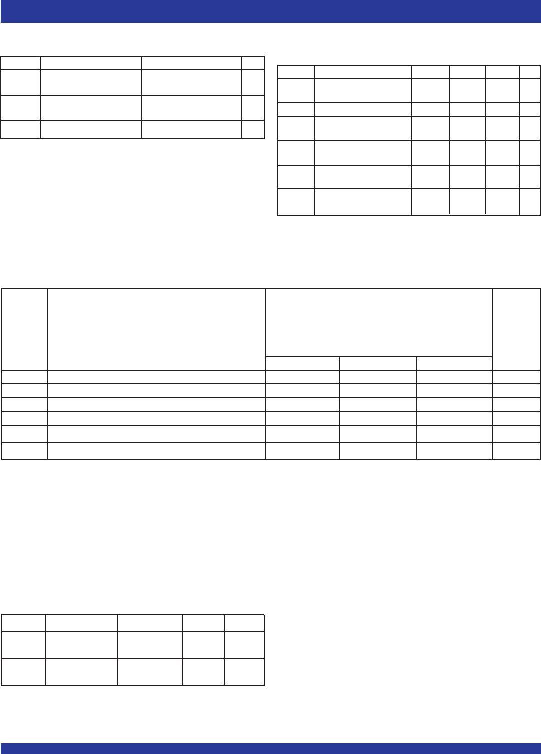
IDT STANDARD MODE
In this mode, the status flags, FF, PAF, HF, PAE, and EF operate in the
manner outlined in Table 1. To write data into to the FIFO, Write Enable
(WEN) must be LOW. Data presented to the DATA IN lines will be clocked
into the FIFO on subsequent transitions of the Write Clock (WCLK). After the
first write is performed, the Empty Flag (EF) will go HIGH. Subsequent
writes will continue to fill up the FIFO. The Programmable Almost-Empty
flag (PAE) will go HIGH after n + 1 words have been loaded into the FIFO,
where n is the Empty Offset value. The default setting for this value is stated
in the footnote of Table 1. This parameter is also user programmable. See
section on Programmable Flag Offset Loading.
If one continued to write data into the FIFO, and we assumed no read
operations were taking place, the Half-Full flag (HF) would toggle to LOW
once the 129th (72V805), 257th (72V815), 513th (72V825), 1,025th
(72V835), and 2,049th (72V845) word respectively was written into the
FIFO. Continuing to write data into the FIFO will cause the Programmable
Almost-Full flag (PAF) to go LOW. Again, if no reads are performed, the
PAF will go LOW after (256-m) writes for the IDT72V805, (512-m) writes for
the IDT72V815, (1,024-m) writes for the IDT72V825, (2,048–m) writes for
the IDT72V835 and (4,096–m) writes for the IDT72V845. The offset “m” is
the Full Offset value. This parameter is also user programmable. See
section on Programmable Flag Offset Loading. If there is no Full Offset
specified, the PAF will be LOW when the device is 31 away from completely
full for IDT72V805, 63 away from completely full for IDT72V815, and 127
away from completely full for the IDT72V825/72V835/72V845.
When the FIFO is full, the Full Flag (FF) will go LOW, inhibiting further
write operations. If no reads are performed after a reset, FF will go LOW
after D writes to the FIFO. D = 256 writes for the IDT72V805, 512 for the
IDT72V815, 1,024 for the IDT72V825, 2,048 for the IDT72V835 and 4,096
for the IDT72V845, respectively.
If the FIFO is full, the first read operation will cause FF to go HIGH.
Subsequent read operations will cause PAF and the Half-Full flag (HF) to
go HIGH at the conditions described in Table 1. If further read operations
occur, without write operations, the Programmable Almost-Empty flag
(PAE) will go LOW when there are n words in the FIFO, where n is the Empty
Offset value. If there is no Empty Offset specified, the PAE will be LOW when
the device is 31 away from completely empty for IDT72V805, 63 away from
completely empty for IDT72V815, and 127 away from completely empty for
IDT72V825/72V835/72V845. Continuing read operations will cause the
FIFO to be empty. When the last word has been read from the FIFO, the EF
will go LOW inhibiting further read operations. REN is ignored when the
FIFO is empty.
FIRST WORD FALL THROUGH MODE (FWFT)
In this mode, the status flags, IR, PAF, HF, PAE, and OR operate in the
manner outlined in Table 2. To write data into to the FIFO, WEN must be
LOW. Data presented to the DATA IN lines will be clocked into the FIFO on
subsequent transitions of WCLK. After the first write is performed, the
Output Ready (OR) flag will go LOW. Subsequent writes will continue to fill
up the FIFO. PAE will go HIGH after n + 2 words have been loaded into the
FIFO, where n is the Empty Offset value. The default setting for this value
is stated in the footnote of Table 2. This parameter is also user program-
mable. See section on Programmable Flag Offset Loading.
If one continued to write data into the FIFO, and we assumed no read
operations were taking place, the HF would toggle to LOW once the 130th
(72V805), 258th (72V815), 514th (72V825), 1,026th (72V835), and 2,050th
(72V845) word respectively was written into the FIFO. Continuing to write
data into the FIFO will cause the PAF to go LOW. Again, if no reads are
performed, the PAF will go LOW after (257-m) writes for the IDT72V805,
(513-m) writes for the IDT72V815, (1,025-m) writes for the IDT72V825,
(2,049–m) writes for the IDT72V835 and (4,097–m) writes for the IDT72V845,
where m is the Full Offset value. The default setting for this value is stated
in the footnote of Table 2.
When the FIFO is full, the Input Ready (IR) flag will go HIGH, inhibiting
further write operations. If no reads are performed after a reset, IR will go
HIGH after D writes to the FIFO. D = 257 writes for the IDT72V805, 513 for
the IDT72V815, 1,025 for the IDT72V825, 2,049 for the IDT72V835 and
4,097 for the IDT72V845. Note that the additional word in FWFT mode is
due to the capacity of the memory plus output register.
If the FIFO is full, the first read operation will cause the IR flag to go LOW.
Subsequent read operations will cause the PAF and HF to go HIGH at the
conditions described in Table 2. If further read operations occur, without
write operations, the PAE will go LOW when there are n + 1 words in the
FIFO, where n is the Empty Offset value. If there is no Empty Offset
specified, the PAE will be LOW when the device is 32 away from completely
empty for IDT72V805, 64 away from completely empty for IDT72V815, and
128 away from completely empty for IDT72V825/72V835/72V845. Continu-
ing read operations will cause the FIFO to be empty. When the last word has
been read from the FIFO, OR will go HIGH inhibiting further read operations.
REN is ignored when the FIFO is empty.
PROGRAMMABLE FLAG LOADING
Full and Empty flag Offset values can be user programmable. The
IDT72V805/72V815/72V825/72V835/72V845 has internal registers for these
offsets. Default settings are stated in the footnotes of Table 1 and Table 2.
Offset values are loaded into the FIFO using the data input lines D0-D11.
To load the offset registers, the Load (LD) pin and WEN pin must be held
LOW. Data present on D0-D11 will be transferred in to the Empty Offset
register on the first LOW-to-HIGH transition of WCLK. By continuing to hold
the LD and WEN pin low, data present on D0-D11 will be transferred into
the Full Offset register on the next transition of the WCLK. The third
transition again writes to the Empty Offset register. Writing all offset
registers does not have to occur at one time. One or two offset registers can
be written and then by bringing the LD pin HIGH, the FIFO is returned to