IDT72V805/72V815/72V825/72V835/72V845
3.3 V CMOS DUAL SyncFIFO™ 256 x 18, 512 x 18, 1,024 x 18, 4,096 x 18
COMMERCIAL AND INDUSTRIAL
TEMPERATURE RANGES
13
NO OPERATION
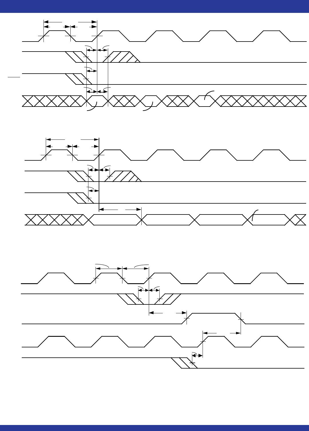
RCLK
REN
EF
t
ENS
t
ENH
VALID DATA
t
OLZ
Q
0
- Q
17
OE
WCLK
WEN
4295 drw 07
t
CLK
t
CLKH
t
CLKL
t
REF
t
REF
t
A
t
OE
t
OHZ
SKEW1
t
(1)
NOTES:
1. tSKEW1 is the minimum time between a rising WCLK edge and a rising RCLK edge to guarantee that EF will go HIGH during the current clock cycle. If the time between
the rising edge of WCLK and the rising edge of RCLK is less than tSKEW1, then EF may not change state until the next RCLK edge.
2. Select this mode by setting (FL, RXI, WXI) = (0,0,0), (0,1,1), (1,0,0) or (1,1,1) during Reset.
WCLK
D
0
- D
17
WEN
RCLK
EF
Q
0
- Q
17
REN
t
DS
t
ENS
t
REF
0
12 3
D
DDD
01
DD
(first valid write)
OE
D
4
t
ENS
4295 drw 08
t
SKEW1
t
FRL
(1)
t
OLZ
t
OE
t
A
t
A
NOTES:
1. When tSKEW1 minimum specification, tFRL (maximum) = tCLK + tSKEW1. When tSKEW1 < minimum specification, tFRL (maximum) = either 2*tCLK + tSKEW1 or tCLK + tSKEW1.
The Latency Timing applies only at the Empty Boundary (EF = LOW).
2. The first word is available the cycle after EF goes HIGH, always.
3. Select this mode by setting (FL, RXI, WXI) = (0,0,0), (0,1,1), (1,0,0) or (1,1,1) during Reset.
Figure 8. First Data Word Latency with Single Register-Buffered EF (IDT Standard Mode)
Figure 7. Read Cycle Timing with Single Register-Buffered EF (IDT Standard Mode)