22
IDT72V805/72V815/72V825/72V835/72V845
3.3 V CMOS DUAL SyncFIFO™ 256 x 18, 512 x 18, 1,024 x 18, 4,096 x 18
COMMERCIAL AND INDUSTRIAL
TEMPERATURE RANGES
NOTES:
1. tSKEW1 is the minimum time between a rising WCLK edge and a rising RCLK edge to guarantee that EF will go HIGH after one RCLK cycle plus tREF. If the time between the rising
edge of WCLK and the rising edge of RCLK is less than tSKEW1. then the EF deassertion may be delayed an extra RCLK cycle.
2. LD = HIGH
3. Select this mode by setting (FL, RXI, WXI) = (0,1,0) or (1,1,0) during Reset.
Figure 26. Read Cycle Timing with Double Register-Buffered EF (IDT Standard Timing)
NO OPERATION
RCLK
REN
EF
t
CLKL
t
ENH
t
REF
LAST WORD
t
A
t
OLZ
t
OE
Q
0
-
Q
17
OE
WCLK
(1)
WEN
4295 drw 26
D
0
-
D
17
t
ENS
t
ENS
t
ENH
t
DS
FIRST WORD
t
OHZ
12
t
CLK
t
CLKH
t
REF
t
SKEW1
t
DH
W
1
W
2
W
4
W
[n +2]
W
[n+3]
WCLK
WEN
D
0
- D
17
RCLK
t
DH
t
DS
t
SKEW1
REN
Q
0
- Q
17
t
DS
t
A
t
REF
OR
W
1
DATA IN OUTPUT REGISTER
(1)
W
3
1
2
3
t
ENH
t
REF
4295 drw 27
t
ENS
NOTES:
1. tSKEW1 is the minimum time between a rising WCLK edge and a rising RCLK edge for OR to go HIGH during the current cycle. If the time between the rising edge of WLCK and the
rising edge of RCLK is less than tSKEW1, then the OR deassertion may be delayed one extra RCLK cycle.
2. LD = HIGH, OE = LOW
3. Select this mode by setting (FL, RXI, WXI) = (0,0,1) or (1,0,1) during Reset.
Figure 27. OR Flag Timing and First Word Fall Through when FIFO is Empty (FWFT mode)
IDT72V805/72V815/72V825/72V835/72V845
3.3 V CMOS DUAL SyncFIFO™ 256 x 18, 512 x 18, 1,024 x 18, 4,096 x 18
COMMERCIAL AND INDUSTRIAL
TEMPERATURE RANGES
23
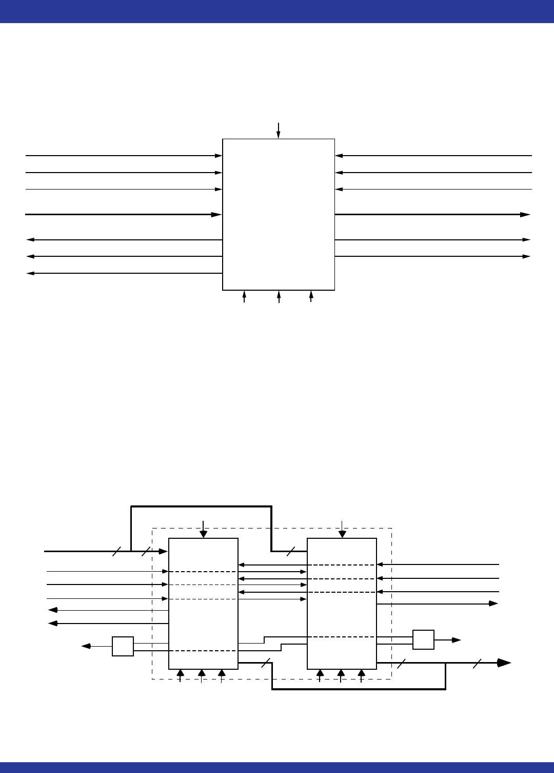
Figure 29. Block Diagram of the Two FIFOs Contained in One IDT72V805/72V815/72V825/72V835/72V845
Configured for a 36-Bit Width Expansion
WRITE CLOCK (WCLK)
WRITE ENABLE (WEN)
READ CLOCK (RCLK)
READ ENABLE (REN)
LOAD (LD)
OUTPUT ENABLE (OE)
DATA IN (D)
DATA OUT (Q)
FULL FLAG/INPUT
READY (FF/IR)
PROGRAMMABLE (PAE)
HALF FULL FLAG (HF)
EMPTY FLAG/OUTPUT
READY (EF/OR)
PROGRAMMABLE (PAF)
RESET (RS)
FIFO A
FIFO B
RESET (RS)
36
36
18 18
18
18
FF/IR EF/OR
4295 drw 29
FL WXI RXI
FL WXI RXI
FF/IR EF/OR
WRITE CLOCK (WCLK)
WRITE ENABLE (WEN)
READ CLOCK (RCLK)
READ ENABLE (REN)
LOAD (LD)
OUTPUT ENABLE (OE)
DATA IN (D
0
- D
17
)
DATA OUT (Q
0
- Q
17
)
FULL FLAG/INPUT READY (FF/IR)
PROGRAMMABLE (PAE)
HALF-FULL FLAG (HF)
EMPTY FLAG/OUTPUT READY (EF/OR)
PROGRAMMABLE (PAF)
RESET (RS)
IDT
72V805
72V815
72V825
72V835
72V845
4295 drw 28
FL RXI WXI
OPERATING CONFIGURATIONS
SINGLE DEVICE CONFIGURATION
Each of the two FIFOs contained in a single IDT72V805/72V815/
72V825/72V835/72V845 may be used as a stand-alone device when the
application requirements are for 256/512/1,024/2,048/4,096 words or less.
These FIFOs are in a single Device Configuration when the First Load (FL),
Write Expansion In (WXI) and Read Expansion In (RXI) control inputs are
configured as (FL, RXI, WXI = (0,0,0), (0,0,1), (0,1,0), (1,0,0), (1,0,1) or
(1,1,0) during reset (Figure 28).
Figure 28. Block Diagram of Single 256 x 18, 512 x 18, 1,024 x 18, 2,048 x 18, 4,096 x 18 Synchronous FIFO
(one of the two FIFOs contained in the IDT72V805/72V815/72V825/72V835/72V845)
NOTE:
1. Do not connect any output control signals directly together.
WIDTH EXPANSION CONFIGURATION
Word width may be increased simply by connecting together the control
signals of FIFO A and B. Status flags can be detected from any one device.
The exceptions are the Empty Flag/Output Ready and Full Flag/Input
Ready. Because of variations in skew between RCLK and WCLK, it is
possible for flag assertion and deassertion to vary by one cycle between
FIFOs. To avoid problems the user must create composite flags by gating
the Empty Flags/Output Ready of every FIFO, and separately gating all Full
Flags/Input Ready. Figure 29 demonstrates a 36-word width by using two
IDT72V805/72V815/72V825/72V835/72V845s. Any word width can be
attained by adding additional IDT72V805/72V815/72V825/72V835/72V845s.
These FIFOs are in a single Device Configuration when the First Load (FL),
Write Expansion In (WXI) and Read Expansion In (RXI) control inputs are
configured as (FL, RXI, WXI = (0,0,0), (0,0,1), (0,1,0), (1,0,0), (1,0,1) or
(1,1,0) during reset (Figure 29). Please see the Application Note AN-83.
24
IDT72V805/72V815/72V825/72V835/72V845
3.3 V CMOS DUAL SyncFIFO™ 256 x 18, 512 x 18, 1,024 x 18, 4,096 x 18
COMMERCIAL AND INDUSTRIAL
TEMPERATURE RANGES
Figure 30. Block Diagram of 8,192 x 18 Synchronous FIFO Memory with Programmable Flags
Used in Depth Expansion Configuration
DEPTH EXPANSION CONFIGURATION — DAISY CHAIN TECHNIQUE
(WITH PROGRAMMABLE FLAGS)
These devices can easily be adapted to applications requiring more than
256/512/1,024/2,048/4,096 words of buffering. Figure 30 shows Depth
Expansion using one IDT72V805/72V815/72V825/72V835/72V845s. Maxi-
mum depth is limited only by signal loading. Follow these steps:
1. The first device must be designated by grounding the First Load (FL)
control input.
2. All other devices must have FL in the HIGH state.
3. The Write Expansion Out (WXO) pin of each device must be tied to the
Write Expansion In (WXI) pin of the next device. See Figure 30.
4. The Read Expansion Out (RXO) pin of each device must be tied to the
Read Expansion In (RXI) pin of the next device. See Figure 30
5. All Load (LD) pins are tied together.
6. The Half-Full flag (HF) is not available in this Depth Expansion
Configuration.
7. EF, FF, PAE, and PAF are created with composite flags by ORing
together every respective flags for monitoring. The composite PAE
and PAF flags are not precise.
8. In Daisy Chain mode, the flag outputs are single register-buffered and
the partial flags are in asynchronous timing mode.
DEPTH EXPANSION CONFIGURATION (FWFT MODE)
In FWFT mode, the FIFOs can be connected in series (the data outputs
of one FIFO connected to the data inputs of the next) with no external logic
necessary. The resulting configuration provides a total depth equivalent to
the sum of the depths associated with each single FIFO. Figure 31 shows
a depth expansion using one IDT72V805/72V815/72V825/72V835/72V845
devices.
Care should be taken to select FWFT mode during Master Reset for all
FIFOs in the depth expansion configuration. The first word written to an
empty configuration will pass from one FIFO to the next (“ripple down”) until
it finally appears at the outputs of the last FIFO in the chain–no read
operation is necessary but the RCLK of each FIFO must be free-running.
Each time the data word appears at the outputs of one FIFO, that device’s
OR line goes LOW, enabling a write to the next FIFO in line.
LOAD
WRITE CLOCK
WRITE ENABLE
READ CLOCK
READ ENABLE
OUTPUT ENABLE
DATA IN DATA OUT
RESET
FIRST LOAD (FL)
Vcc
WXOA
WXIA
RXOA
RXIA
WXOB
WXIB
RXOB
RXIB
IDT72V845
FFA/IRA
PAFA
EFA/ORA
PAEA
PAFB
PAEB
EF
PAE
FF
PAF
4295 drw 30
RCLKB
RENB
OEB
WCLKB
WENB
RSB
FLA
RCLKA
RENA
OEA
WCLKA
WENA
RSA
LDA
DAn
QAn
DBn
QBn
LDB
FIFO A
4,096 x 18
FIFO B
4,096 x 18
FFA/IRA EFA/ORA

72V815L10PF

Mfr. #:
Manufacturer:
Description:
FIFO 3.3V 1KX18 SYNC FIFO
Lifecycle:
New from this manufacturer.
Delivery:
DHL FedEx Ups TNT EMS
Payment:
T/T Paypal Visa MoneyGram Western Union