LTC4310-1/LTC4310-2
1
431012fa
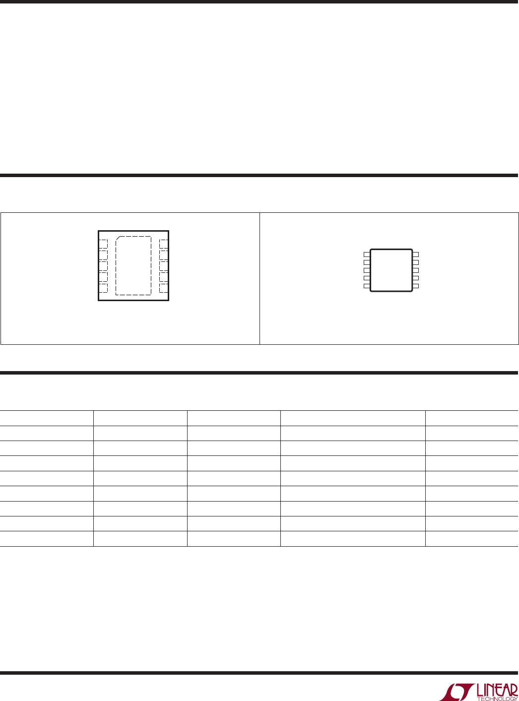
Typical applicaTion
DescripTion
Hot-Swappable
I
2
C Isolators
The LTC
®
4310 provides bidirectional I
2
C communications
between two I
2
C buses whose grounds are isolated from
one another. Each LTC4310 encodes I
2
C bus logic states
into signals that are transmitted across an isolation barrier
to another LTC4310. The receiving LTC4310 decodes the
transmission and drives its l
2
C bus to the appropriate logic
state. The isolation barrier can be bridged by an inexpensive
Ethernet, or other transformer, to achieve communications
across voltage differences reaching thousands of volts, or
it can be bridged by capacitors for lower voltage isolation.
The LTC4310-1 is intended for use in 100kHz I
2
C systems.
The LTC4310-2 is intended for 400kHz I
2
C systems.
Rise time accelerators provide strong pull-up currents on
SCL and SDA rising edges to meet rise time specifications
for heavily loaded systems. Data and clock Hot Swap™
circuitry prevent data corruption when a card is inserted
into or removed from a live bus. When a bus is stuck low
for 37ms, the LTC4310 turns off its pull-down devices
and generates up to sixteen clocks and a STOP bit in an
attempt to free the bus. Driving EN low sets the LTC4310
in a very low current shutdown mode to conserve power.
L, LT, LTC, LTM, Linear Technology and the Linear logo are registered trademarks of Linear
Technology Corporation. Hot Swap is a trademark of Linear Technology Corporation. All other
trademarks are the property of their respective owners.
1500V Isolated I
2
C System
FeaTures
applicaTions
n
Bidirectional I
2
C Communication Between Two
Isolated Buses
n
Full Isolation with Inexpensive Ethernet
Transformers or Capacitors
n
Low Voltage Level Shifting
n
I
2
C Maximum Operating Frequency:
100kHz for LTC4310-1
400kHz for LTC4310-2
n
I
2
C Specification Compliant V
OL
, V
IL
n
±5kV Human Body Model ESD Protection
n
Rise Time Accelerators
n
SDA, SCL Hot-Swapping
n
Very Low Shutdown Current
n
Stuck Bus Disconnect and Recovery
n
Thermal Shutdown
n
10-Lead MSOP and 3mm × 3mm DFN Packages
n
Isolated I
2
C, SMBus and PMBus Interfaces
n
Isolated Power Supplies
n
Positive-to-Negative Rail Communications
n
Power-over-Ethernet
LTC4310 Operating Through
20kV/µs Common Mode Transient
RXP
10/100Base-TX
ETHERNET TRANSFORMER
EPF8119S
RXN
TXP
SDA
SCL
EN
TXN GND
READY
0.01µF0.01µF
ISOLATED
5V
3.3V
3.3k 3.3k3.3k 3.3k
LTC4310-1
V
CC
SDA2
SCL2
SDA1
SCL1
0.01µF
0.01µF
431012 TA01a
TXP
TXN
RXP
RXN
SDA
SCL
EN
READY
GND
LTC4310-1
V
CC
2µs/DIV
20kV/µs
0V
0V
500V/
DIV
2V/DIV
431012 TA01b
SDA
SCL
LTC4310-1/LTC4310-2
2
431012fa
absoluTe MaxiMuM raTings
Input Supply Voltage (V
CC
) .......................... –0.3V to 6V
Input and Bidirectional Pin Voltages
SCL, SDA, EN, RXP, RXN .......................... –0.3V to 6V
Output Voltages
READY ..................................................... –0.3V to 6V
TXP, TXN ...................... –0.3V to V
CC
+ 0.3V (6V Max)
Maximum Sink Current (SDA, SCL, READY) ..........30mA
(Notes 1, 4)
TOP VIEW
DD PACKAGE
10-LEAD (3mm × 3mm) PLASTIC DFN
10
11
GND
9
6
7
8
4
5
3
2
1
RXN
RXP
V
CC
TXP
TXN
EN
SDA
SCL
READY
GND
T
JMAX
= 125°C, θ
JA
= 43°C/W
EXPOSED PAD (PIN 11) PCB CONNECTION TO GROUND IS OPTIONAL
1
2
3
4
5
EN
SDA
SCL
READY
GND
10
9
8
7
6
RXN
RXP
V
CC
TXP
TXN
TOP VIEW
MS PACKAGE
10-LEAD PLASTIC MSOP
T
JMAX
= 150°C, θ
JA
= 120°C/W
pin conFiguraTion
orDer inForMaTion
LEAD FREE FINISH TAPE AND REEL PART MARKING* PACKAGE DESCRIPTION TEMPERATURE RANGE
LTC4310CDD-1#PBF LTC4310CDD-1#TRPBF LFCH 10-Lead (3mm × 3mm) Plastic DFN 0°C to 70°C
LTC4310IDD-1#PBF LTC4310IDD-1#TRPBF LFCH 10-Lead (3mm × 3mm) Plastic DFN –40°C to 85°C
LTC4310CMS-1#PBF LTC4310CMS-1#TRPBF LTFCG 10-Lead Plastic MSOP 0°C to 70°C
LTC4310IMS-1#PBF LTC4310IMS-1#TRPBF LTFCG 10-Lead Plastic MSOP –40°C to 85°C
LTC4310CDD-2#PBF LTC4310CDD-2#TRPBF LFCK 10-Lead (3mm × 3mm) Plastic DFN 0°C to 70°C
LTC4310IDD-2#PBF LTC4310IDD-2#TRPBF LFCK 10-Lead (3mm × 3mm) Plastic DFN –40°C to 85°C
LTC4310CMS-2#PBF LTC4310CMS-2#TRPBF LTFCJ 10-Lead Plastic MSOP 0°C to 70°C
LTC4310IMS-2#PBF LTC4310IMS-2#TRPBF LTFCJ 10-Lead Plastic MSOP –40°C to 85°C
Consult LTC Marketing for parts specified with wider operating temperature ranges. *The temperature grade is identified by a label on the shipping container.
For more information on lead free part marking, go to: http://www.linear.com/leadfree/
For more information on tape and reel specifications, go to: http://www.linear.com/tapeandreel/
Operating Ambient Temperature Range
LTC4310C ................................................ 0°C to 70°C
LTC4310I.............................................. –40°C to 85°C
Storage Temperature Range
DD ..................................................... –65°C to 125°C
MS ..................................................... –65°C to 150°C
Lead Temperature (Soldering, 10 sec)
MS Package ...................................................... 300°C
LTC4310-1/LTC4310-2
3
431012fa
elecTrical characTerisTics
SYMBOL PARAMETER CONDITIONS MIN TYP MAX UNITS
Supplies
V
CC
Input Supply Range
l
3 5.5 V
I
CC
Input Supply Current, LTC4310-1
Input Supply Current, LTC4310-2
EN = V
CC
= 5.5V, SDA = SCL = V
SDA,SCL(OL)
EN = V
CC
= 5.5V, SDA = SCL = V
SDA,SCL(OL)
l
l
6.5
7
8
8.5
mA
mA
I
CC(SD)
Shutdown Input Supply Current EN = 0V, V
CC
= 5.5V
l
0.1 ±10 µA
V
CCH(UVL)
Input Supply Undervoltage Lockout
Rising Threshold Voltage
l
2.1 2.4 2.7 V
V
CC(UVL, HYST)
Input Supply Undervoltage Lockout
Hysteresis
l
90 190 270 mV
I
2
C Interface
V
SDA,SCL(OL)
SDA, SCL Logic Low Output Voltage I
(SDA,SCL)
= 4mA, 500µA; V
CC
= 3V, 5.5V
l
310 350 380 mV
V
SDA,SCL(IL,R)
SDA, SCL Controlled Rising Edge Rate
Turn-Off Threshold Voltage
V
CC
= 3V, 5.5V (Note 5)
l
0.3 • V
CC
0.35 • V
CC
0.4 • V
CC
V
V
SDA,SCL(IL,F)
SDA, SCL Logic Low Falling Input
Threshold Voltage
V
CC
= 3V
l
0.4 • V
CC
0.45 • V
CC
0.5 • V
CC
V
I
SDA,SCL(OH)
SDA, SCL Input Current SDA = SCL = 5.5V; V
CC
= 0V, 5.5V
l
0 ±5 µA
I
2
C Interface Timing
dV/dt
RISE
Bus Line Controlled Rising Edge Rate,
LTC4310-1
0.35V < V
BUS
< 0.35 • V
CC
, V
CC
= 3V
0.35V < V
BUS
< 0.35 • V
CC
, V
CC
= 5.5V
l
l
0.8
1.5
1.16
2.14
1.4
2.6
V/µs
V/µs
Bus Line Controlled Rising Edge Rate,
LTC4310-2
0.35V < V
BUS
< 0.35 • V
CC
, V
CC
= 3V
0.35V < V
BUS
< 0.35 • V
CC
, V
CC
= 5.5V
l
l
2
3.9
3
5.4
3.9
6.9
V/µs
V/µs
t
PHL(SDA,SCL)
SDA, SCL High-to-Low Propagation
Delay
V
CC
= 5.5V (Note 3)
l
170 270 ns
f
SCL(MAX)
Maximum SCL Clock Frequency LTC4310-1
LTC4310-2
l
l
100
400
kHz
kHz
C
IN
SCL, SDA Input Capacitance SCL, SDA = V
CC
(Note 2) 10 pF
Rise Time Accelerators
V
BOOST
SDA, SCL Rise Time Accelerator
Activation Threshold Voltage
V
CC
= 3V (Note 5)
l
0.32 • V
CC
0.45 • V
CC
0.5 • V
CC
V
I
BOOST
SDA, SCL Rise Time Accelerator
Current
V
CC
= 3V
l
2 6 mA
READY Open-Drain Output
V
READY(OL)
READY Output Low Voltage I
READY
= 4mA
l
50 400 mV
I
READY(OH)
READY Off-Current READY= V
CC
= 5.5V, EN = 0V
l
0.1 ±10 µA
Connection Control
V
EN,RISE
EN Rising Threshold Voltage
l
0.6 • V
CC
0.9 • V
CC
V
V
EN,FALL
EN Falling Threshold Voltage
l
0.1 • V
CC
0.3 • V
CC
V
I
EN(OH)
EN Input Current EN = V
CC
= 5.5V
l
0.1 ±10 µA
t
IDLE
Bus Idle Time
l
75 115 155 µs
t
UVLO,EN_FILT
Start-Up Filter Time
l
700 900 1200 µs
t
STUCK
SDA, SCL Bus Stuck Low Disconnect
l
27 37 47 ms
The l denotes the specifications which apply over the full operating
temperature range, otherwise specifications are at T
A
= 25°C. V
CC
= 3.3V, unless otherwise noted.

LTC4310IMS-1#TRPBF

Mfr. #:
Manufacturer:
Analog Devices Inc.
Description:
Digital Isolators I2C Isolater, 100kHz Max Bus Frequency
Lifecycle:
New from this manufacturer.
Delivery:
DHL FedEx Ups TNT EMS
Payment:
T/T Paypal Visa MoneyGram Western Union