LTC4310-1/LTC4310-2
4
431012fa
SYMBOL PARAMETER CONDITIONS MIN TYP MAX UNITS
t
MAX(TX)
Maximum Time Between TXP, TXN
Transmit Events
l
0.85 1.15 1.45 ms
t
MAX(RX)
Maximum Time Between RXP, RXN
Receive Events
l
3.4 4.6 5.8 ms
Transmit Outputs
V
TX(OL)
TXP, TXN Single-Ended Output Low I
SINK
= 100µA, V
CC
= 3V
l
1.5 5 mV
V
TX(OH)
TXP, TXN Single-Ended Output High 15kΩ to GND on TXP, TXN; V
CC
= 3V, 5.5V
l
0.95 1.25 1.52 V
t
R(TX)
TXP, TXN Output Rise Time C
TXP
, C
TXN
= 20pF
l
1 3 ns
t
F(TX)
TXP, TXN Output Fall Time C
TXP
, C
TXN
= 20pF
l
1 3 ns
t
PWMIN(TX)
TXP, TXN Minimum Transmission
Pulse Width
V
CC
= 3V, 5.5V
l
31.5 35 39 ns
Receive Inputs
V
RX(TH)
RXP, RXN Differential High Level
Threshold
RXP, RXN Pins; V
CC
= 3V, 5.5V
l
0.3 0.5 0.875 V
t
PWMIN(RX)
RXP, RXN Minimum Received Pulse
Width
V
CC
= 3V, 5.5V
l
30 ns
R
RX(IN)
RXP, RXN Differential Input Resistance
l
13 16.5 20
elecTrical characTerisTics
The l denotes the specifications which apply over the full operating
temperature range, otherwise specifications are at T
A
= 25°C. V
CC
= 3.3V, unless otherwise noted.
Note 1: Stresses beyond those listed under Absolute Maximum Ratings
may cause permanent damage to the device. Exposure to any Absolute
Maximum Rating condition for extended periods may affect device
reliability and lifetime.
Note 2. Guaranteed by design, not tested in production.
Note 3. SDA, SCL high-to-low propagation delay is measured from the
beginning of a new received message telling the LTC4310 to drive its SDA,
SCL pins from high to low, to when the SDA, SCL lines have fallen below
0.5 • V
CC
. It includes approximately 87ns required for an LTC4310 to
receive a message on the RXP and RXN pins, plus the time the LTC4310
requires to process the message and pass the low to the data and clock
buffers, plus the time required by the buffers to drive their bus pins below
0.5 • V
CC
.
Note 4. All currents into pins are positive, all voltages are referenced to
GND unless otherwise specified.
Note 5. Internal control circuitry prevents the rise time accelerators from
activating until the rising edge rate control circuitry is off.
LTC4310-1/LTC4310-2
5
431012fa
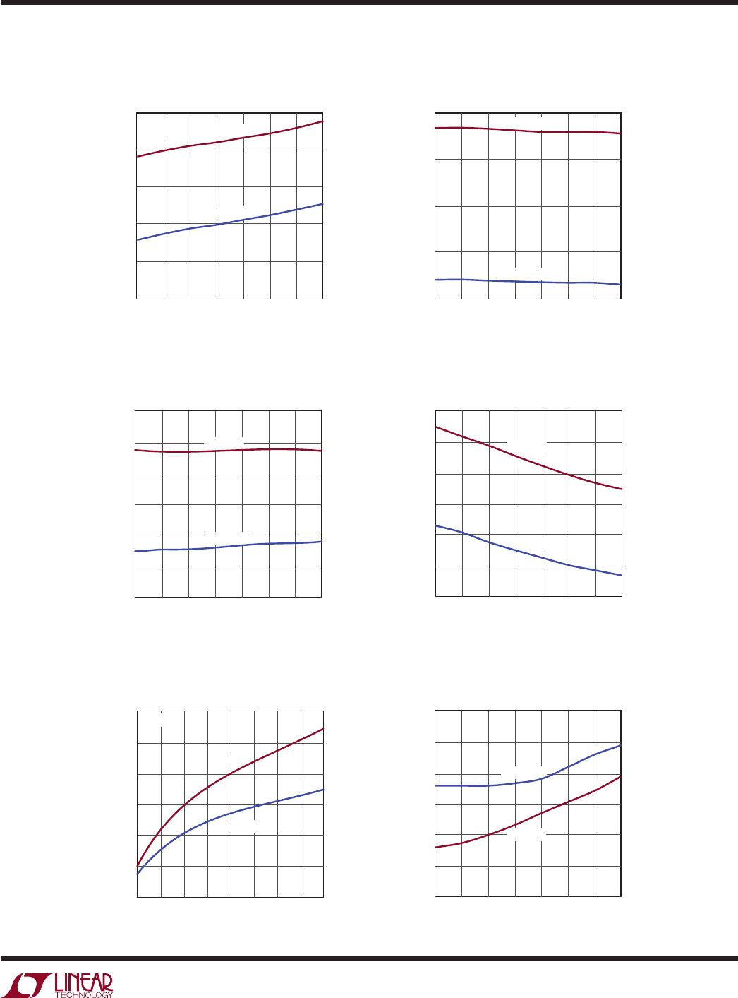
Typical perForMance characTerisTics
SDA, SCL Controlled Rising Edge
Rate vs Temperature, LTC4310-1
SDA, SCL Controlled Rising Edge
Rate vs Temperature, LTC4310-2
SDA, SCL Rise Time Accelerator
Pull-Up Current vs Temperature
SDA, SCL Rise Time Accelerator
Pull-Up Current vs Bus Capacitance
SDA,SCL Falling Propagation
Delay vs Temperature
I
CC
vs Temperature, LTC4310-1
TEMPERATURE (°C)
–50
I
CC
(mA)
4.8
5.0
4.6
4.4
0 25 75
–25
50 100 125
4.2
4.0
431012 G01
V
CC
= 3.3V
V
CC
= 5V
SDA = 0V
SCL = V
CC
TEMPERATURE (°C)
–50
CONTROLLED RISE RATE (V/µs)
1.6
1.8
1.4
1.2
0 25 75
–25
50 100 125
2.0
431012 G02
V
CC
= 3.3V
V
CC
= 5V
TEMPERATURE (°C)
–50
CONTROLLED RISE RATE (V/µs)
4.5
5.0
4.0
3.5
0 25 75
–25
50 100 125
3.0
2.5
5.5
431012 G03
V
CC
= 3.3V
V
CC
= 5V
TEMPERATURE (°C)
–50
PULL-UP CURRENT (mA)
9
10
8
7
0 25 75
–25
50 100 125
6
5
11
431012 G04
V
CC
= 3.3V
V
CC
= 5V
BUS CAPACITANCE (pF)
0
PULL-UP CURRENT (mA)
8
10
6
4
200 300 500
100
400 600 700 800
2
0
12
431012 G05
V
CC
= 3.3V
V
CC
= 5V
T
A
= 25°C
TEMPERATURE (°C)
–50
PROPAGATION DELAY (ns)
180
200
160
140
0 25 75
–25
50 100 125
120
0
220
431012 G06
V
CC
= 3.3V
V
CC
= 5V
LTC4310-1/LTC4310-2
6
431012fa
pin FuncTions
EN (Pin 1): Device Enable Input. Pulling EN up to V
CC
sets the device in normal operation mode, allowing bus
information to be sent and received across the barrier.
Grounding EN disables communication across the bar-
rier and debiases all internal circuitry, setting the device
in a very low current shutdown mode. Connect to V
CC
if
unused.
SDA (Pin 2): Serial Bus Data Input/Output. This is the
bidirectional data line for the two-wire bus. An external
pull-up resistor or current source from SDA to a supply
voltage greater than or equal to the V
CC
voltage is required.
See the Applications Information section for guidance
on selecting the resistor or current source value. Do not
leave open.
SCL (Pin 3): Serial Bus Clock Input/Output. This is the
bidirectional clock line for the two-wire bus. An external
pull-up resistor or current source from SCL to a supply
voltage greater than or equal to the V
CC
voltage is required.
See the Applications Information section for guidance
on selecting the resistor or current source value. Do not
leave open.
READY (Pin 4): Device Receiving Indicator Output. READY
is an open-drain digital output that pulls low when the
LTC4310 is driving its SDA and SCL pins with the logic
state information it is receiving on its RXP and RXN pins.
Connect this pin to V
CC
with a 10k resistor. This pin can
be left open or tied to GND if unused.
GND (Pin 5): Device Ground.
TXN (Pin 6): Negative Transmit Output. Tie TXN to the
negative side of the transformer primary winding or to the
RXN pin of another LTC4310 through a ceramic capacitor.
See the Applications Information section for guidance in
selecting the capacitor value. Do not leave open.
TXP (Pin 7): Positive Transmit Output. Tie TXP to the
positive side of the transformer primary winding or to the
RXP pin of another LTC4310 through a ceramic capacitor.
See the Applications Information section for guidance in
selecting the capacitor value. Do not leave open.
V
CC
(Pin 8): Device Power Supply Input. Connect a by-
pass capacitor of at least 0.01µF directly between V
CC
and GND.
RXP (Pin 9): Positive Receive Input. Tie RXP to the posi-
tive side of the transformer secondary winding or to the
TXP pin of another LTC4310 through a ceramic capacitor.
See the Applications Information section for guidance in
selecting the capacitor value. Do not leave open.
RXN (Pin 10): Negative Receive Input. Tie RXN to the nega-
tive side of the transformer secondary winding or to the
TXN pin of another LTC4310 through a ceramic capacitor.
See the Applications Information section for guidance in
selecting the capacitor value. Do not leave open.
Exposed Pad (Pin 11) DFN Package Only: The exposed
pad may be left open or connected to device ground.

LTC4310IMS-1#TRPBF

Mfr. #:
Manufacturer:
Analog Devices Inc.
Description:
Digital Isolators I2C Isolater, 100kHz Max Bus Frequency
Lifecycle:
New from this manufacturer.
Delivery:
DHL FedEx Ups TNT EMS
Payment:
T/T Paypal Visa MoneyGram Western Union