LTC4310-1/LTC4310-2
13
431012fa
Once a STOP bit or bus idle occurs on both the local and
isolated buses, the LTC4310 reactivates its buffers and
rise time accelerators.
READY Digital Output
The READY pin provides a digital output flag that pulls
low to indicate that the LTC4310 is driving its SDA and
SCL pins with the logic state information it is receiving on
its RXP and RXN pins from the other LTC4310. READY is
driven by an N-channel MOSFET open-drain pull-down that
is capable of sinking 4mA while holding 0.4V maximum.
The pull-down turns off whenever the LTC4310 is not
driving its SDA and SCL pins—during start-up, thermal
shutdown, low current shutdown and after disconnection
due to a stuck bus or failure to receive a transmission
within 4.6ms. Connect a resistor to the bus pull-up supply
to provide the pull-up.
Design Example: High Voltage Isolation Using an
Inexpensive Ethernet Transformer
Figure 1 shows the LTC4310-1 providing I
2
C communi-
cations between two buses whose ground voltages can
differ up to 1500V. An EPF8119S Ethernet transformer is
used to bridge the isolation barrier. The left I
2
C bus con-
nects to the LTC4310-1 and two other devices, resulting
in a bus parasitic capacitance of 40pF in this example
set-up. Referring to the V
CC
= 3.3V curve in Figure 2,
7.5k pull-up resistors are chosen for R1 and R2. The right
I
2
C bus connects to another LTC4310-1 and four slave
devices, resulting in a bus parasitic capacitance of 80pF.
Referring to the V
CC
= 5V curve in Figure 2, 7.5k pull-up
resistors are also chosen for R5 and R6. Standard 5%
resistors are used.
Sudden changes in the ground differential across the
isolation barrier can be effectively resisted by tying the
center tap of the receive side of the transformer to the
local ground through a 0.01µF capacitor, as shown by
capacitors C2 and C3.
Figure 7 shows the same application as Figure 1, but with
each LTC4310-1 replaced by an LTC4310-2, so that the
bus can switch at frequencies up to 400kHz. To meet the
requirements shown in the curves of Figure 3, R1 and R2
are changed from 7.5k to 4.3k, and R5 and R6 are changed
from 7.5k to 3.3k.
applicaTions inForMaTion
Figure 7. The LTC4310-2 in a 400kHz Application
EPF8119S
C1
0.01µF
C4
0.01µF
3.3V
R1
4.3k
R2
4.3k
R5
3.3k
R6
3.3k
. . .
SLAVE SLAVE#1
SCL1 SCL2
C3
0.01µF
C2
0.01µF
431012 F07
TXP
TXN
RXP
RXN
SDA
SCL
READY
GND GND
RXP
RXN
TXP
TXN
READY
LTC4310-2
LTC4310-2
V
CC
EN
SDA
SCL
V
CC
EN
µP SLAVE#4
R3
10k
R4
10k
IS0LATED
5V
10/100Base-TX
ETHERNET
TRANSFORMER
C
BUS
= 40pF
C
BUS
= 80pF
1
3
6
7
8
16
15
14
11
9
LTC4310-1/LTC4310-2
14
431012fa
applicaTions inForMaTion
TYPICAL APPLICATIONS
Figure 8 shows the LTC4310-1 providing I
2
C communica-
tions between an I
2
C bus referenced to system ground and
an I
2
C bus using –5V for its ground reference. Ceramic
coupling capacitors, C1-C5, are used to bridge the isolation
barrier. This circuit is recommended for ground isolation
voltages less than 100V and is limited by the voltage rating
of C1-C5. Higher voltage ceramic capacitors may be used
to achieve higher isolation voltages. Because the LTC4310
uses a pseudo-differential transmit scheme, capacitor C5
must be connected between ground and –5V to provide a
return path for the transmitted current.
Figure 9 shows the LTC4310-1 in an application circuit
using its zero current shutdown mode. A microprocessor
only activates the left LTC4310-1 when it needs to com-
municate with the isolated I
2
C bus. Because the LTC4310-1
contains a STOP bit and bus idle detection circuitry, there
is no danger of connecting in the middle of a message
when the microprocessor asynchronously reenables the
LTC4310-1.
Figure 8. Low Voltage I
2
C Isolation Between a Ground Referenced Bus and a –5V Referenced Bus
3.3V
C
BUS
= 30pFC
BUS
= 100pF
R1
5.1k
R2
5.1k
R3
10k
431012 F08
C7
0.01µF
C1
–5V
–5V
R5
10k
R6
10k
GND
RXP
RXN
TXP
TXN
LTC4310-1
V
CC
READY
EN
SDA
SCL
R4
10k
C3
C2
C4
C6
0.01µF
GND
TXP
TXN
RXP
RXN
LTC4310-1
V
CC
READY
EN
SDA
SCL
C5
C1 TO C5 = 47pF, 100V
Figure 9. The LTC4310-1 in a Zero Current Shutdown Application
5V
R1
3.3k
R2
3.3k
R3
10k
431012 F09
C7
0.01µF
–5V
–5V
R5
5.1k
R6
5.1k
GND
RXP
RXN
TXP
TXN
LTC4310-1
V
CC
READY
EN
SDA
SCL
R4
10k
C6
0.01µF
GND
TXP
TXN
RXP
RXN
LTC4310-1
V
CC
READY
EN
SDA
SCL
. . .
SLAVE#1
µP
SLAVE#N
ON
OFF
C1
C3
C2
C4
C5
C1 TO C5 = 47pF, 100V
C
BUS
= 150pFC
BUS
= 200pF
LTC4310-1/LTC4310-2
15
431012fa
applicaTions inForMaTion
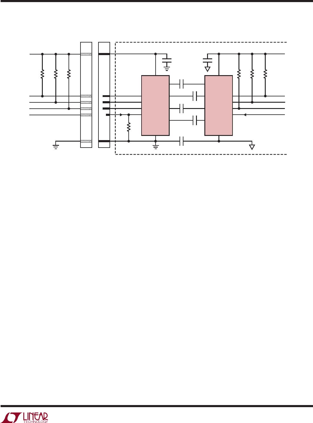
Figure 10. The LTC4310-1 in an I
2
C Hot-Swapping Application
5V
BACKPLANE
CONNECTOR
BACKPLANE
CARD
CONNECTOR
R1
2k
R2
2k
R3
10k
I/O PERIPHERAL CARD
431012 F10
C7
0.01µF
R5
6.8k
R6
10k
R7
100k
GND
RXP
RXN
TXP
TXN
LTC4310-1
V
CC
READY
EN
SDA
SCL
READY
EN
SDA
SCL
READY2
EN2
SDA2
3.3V
SCL2
R4
6.8k
C6
0.01µF
GND
TXP
TXN
RXP
RXN
LTC4310-1
V
CC
READY
EN
SDA
SCL
C1
C3
C2
C4
C5
C1 TO C5 = 47pF, 100V
C
BUS
= 50pFC
BUS
= 400pF
Figure 10 shows the LTC4310-1 in a two-wire bus Hot Swap
application. Using a staggered connector, make EN the
shortest length pin to ensure that the transients associated
with hot swapping have settled before the LTC4310-1 can
be enabled. After connection is complete, a master on the
backplane may drive EN high to bring the LTC4310-1 out
of shutdown mode and into normal operation. Due to its
STOP bit and bus idle detection circuitry, the LTC4310-1’s
driver circuitry is not activated until transactions on both
buses are complete.
LTC4310 Compatibility with Other LTC Bus Buffers
The LTC4310 cannot be used on the same I
2
C bus with the
LTC4300A-1, LTC4303 or LTC4307. During rising edges,
the rise time accelerators of these buffers turn on before
the LTC4310 disables its rise rate regulation circuitry,
resulting in nonmonotonic bus edges.
The LTC4310-1 is compatible with the LTC4301 and
LTC4301L. It is also compatible with the LTC4302, LTC4304,
LTC4305 and LTC4306, provided that the rise time accelera-
tors of these buffers are permanently disabled. All of the
previously mentioned buffers are incompatible with the
LTC4310-2 because the compensation networks of these
buffers cause the bus to rise more slowly than (0.35
V
CC
)/300ns, therefore the LTC4310-2 would not be able
to control the bus rise rate.
LTC4310-1 Compatibility with LTC4310-2
In a typical application such as shown in Figure 1, an
LTC4310-1 can be used on one bus and an LTC4310-2 can
be used on the other, provided that the bus pull-up resis-
tors connected to the LTC4310-1 meet the requirements
of Figure 2, and the bus pull-up resistors connected to the
LTC4310-2 meet the requirements of Figure 3. However,
the bus switching frequency is limited by the rise rate
regulation circuitry of the LTC4310-1. In addition, significant
skew is introduced on the rising edges due to the large
difference in the controlled rise rates of the two buses. For
this reason, it is recommended to use two LTC4310-1’s
in SMBus and standard mode I
2
C applications and to use
two LTC4310-2’s in fast mode I
2
C applications.
The LTC4310-1 cannot be used on the same physical I
2
C
bus with the LTC4310-2, because the LTC4310-1’s rise
rate regulation circuitry controls the bus rise rate to (0.35
V
CC
)/900ns, therefore the LTC4310-2 would not be able
to control the bus rise rate.

LTC4310IMS-1#TRPBF

Mfr. #:
Manufacturer:
Analog Devices Inc.
Description:
Digital Isolators I2C Isolater, 100kHz Max Bus Frequency
Lifecycle:
New from this manufacturer.
Delivery:
DHL FedEx Ups TNT EMS
Payment:
T/T Paypal Visa MoneyGram Western Union