LTC4310-1/LTC4310-2
8
431012fa
operaTion
The LTC4310 provides fully bidirectional communications
between two I
2
C or SMBus buses whose grounds are
isolated from one another. Clock stretching, clock syn-
chronization, arbitration and data acknowledging all work
seamlessly across the barrier, regardless of the locations
of the master(s) and slave(s).
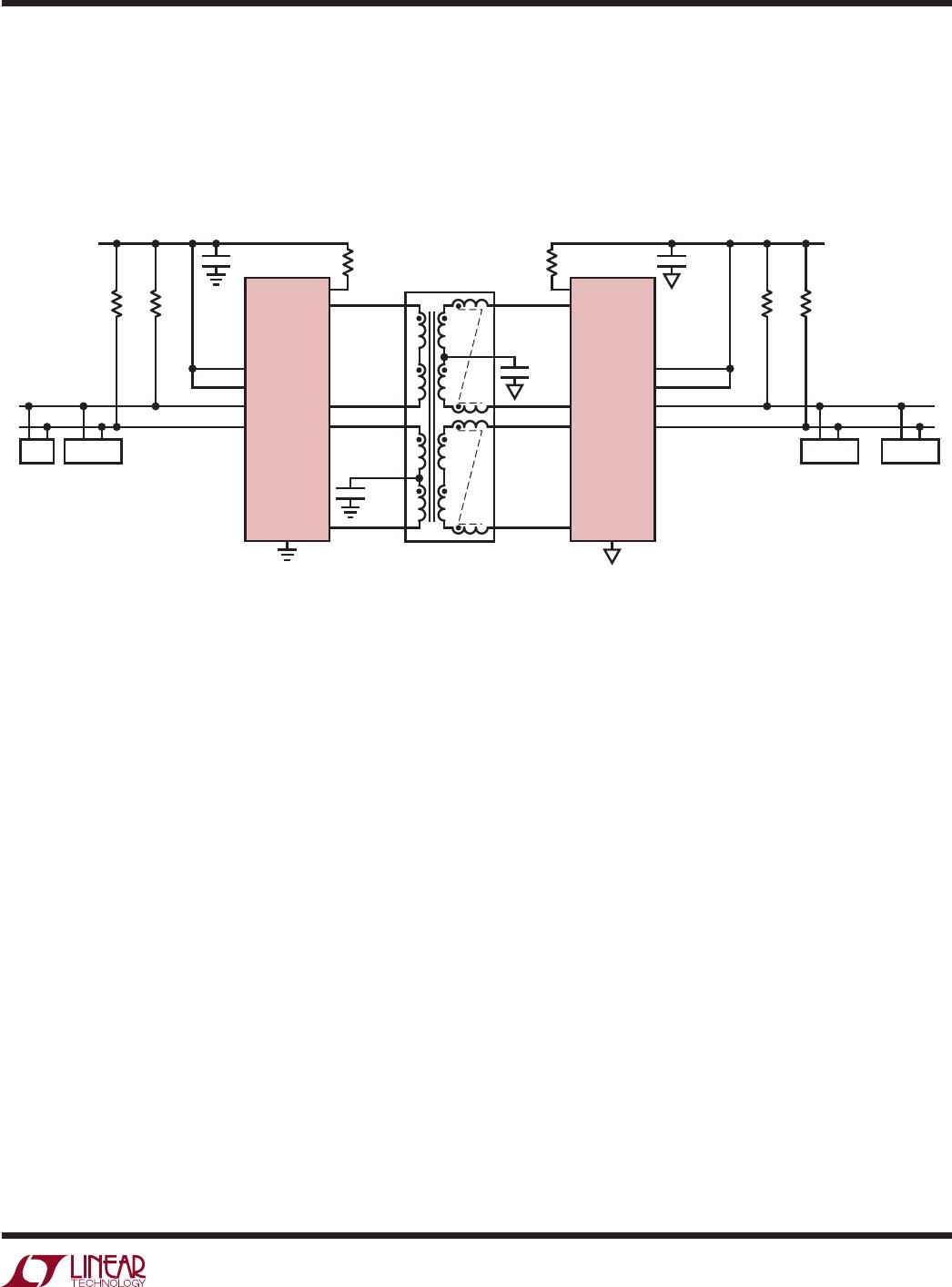
Referring to the application circuit shown in Figure 1, an
LTC4310 is located on each side of the isolation barrier.
Each LTC4310 contains logic detection circuitry that can
differentiate externally driven SDA and SCL logic signals
from its own output signals. Each LTC4310 converts the
logic state of the externally driven signals into a sequence
of pulses that are then transmitted across the isolation bar-
rier via an Ethernet transformer (or coupling capacitors for
low isolation voltage applications) to the other LTC4310.
Each LTC4310 also receives and decodes corresponding
pulses from the other LTC4310 and drives its SDA and
SCL pins accordingly.
Transmissions occur on the TXP and TXN pins in a sequence
of 1.25V pulses. The LTC4310 receives messages on its
RXP and RXN pins. Signals having less than 500mV dif-
ferential voltages are rejected to provide noise immunity
against common-mode transients.
When the LTC4310 receives a message to drive SDA low,
it regulates SDA to 0.35V. If an external device pulls SDA
below 0.35V during this time, the LTC4310 detects this
condition and immediately transmits a LOW to the other
LTC4310.
When an external pull-down device drives SDA below
0.45 • V
CC
from a logic high, TXP and TXN transmit a
message across the isolation barrier instructing the other
LTC4310 to drive its SDA line low.
When the external pull-down device turns off and SDA is
rising between 0V and 0.35 • V
CC
, the LTC4310 limits the
bus rise rate to dV/dt
RISE
via the rise rate limiter circuitry.
It also transmits a high to the other LTC4310. If the SDA
rise rate falls below the threshold, it is assumed that an-
other pull-down on the bus has turned on and is pulling
SDA low, and a command to pull the far side low is sent
across the isolation barrier.
When SDA rises above 0.35 • V
CC
, the rise rate limiter
circuitry is deactivated. When SDA rises above 0.45 • V
CC
,
the rise time accelerator current I
BOOST
is activated, which
provides a strong, slew-limited pull-up current to reduce
system rise time.
The LTC4310 contains power-on reset (POR) circuitry that
sets the data and clock pins in a high impedance state and
deactivates the transmit and receive circuitry until the EN
voltage is high, the device is not in thermal shutdown
and the V
CC
voltage is above the 2.4V UVLO threshold
voltage. The LTC4310 enters thermal shutdown when the
die temperature exceeds 150°C. Grounding EN sets the
LTC4310 in a near-zero current mode.
After the LTC4310 exits POR, STOP bit and bus idle detector
circuitry monitors the logic state of its own SDA and SCL
bus and of the other I
2
C bus in the system via RXP and
RXN. When a STOP bit or bus idle occurs simultaneously
on both I
2
C buses, the LTC4310 activates its SDA and SCL
drivers, logic detection circuitry and rise time accelerators
and drives READY low.
The stuck bus timer and recovery circuitry disable the
SDA and SCL driver, logic detection circuitry and rise
time accelerators if the bus is low for 37ms. A stuck bus
also causes READY to be released high. If the stuck bus
releases high, the I
2
C driver and accelerator circuitry are
reactivated when a STOP bit or bus idle occurs simultane-
ously on both I
2
C buses, as previously described.
(LTC4310 refers to both LTC4310-1 and LTC4310-2)