LTC4310-1/LTC4310-2
10
431012fa
SDA, SCL Bus Pull-Up Resistor Value Selection
When the SDA (or SCL) bus is rising between 0V and
0.35 V
CC
, the LTC4310 controls the bus rise rate to
(0.35 V
CC
)/900ns for the LTC4310-1 and to (0.35 V
CC
)/
300ns for the LTC4310-2. Users must quantify their
parasitic bus capacitance, C
BUS
, and choose a bus pull-
up resistor, R
BUS
, based on their bus pull-up supply
voltage and maximum bus switching frequency to en-
sure that each bus rises faster than the controlled rise
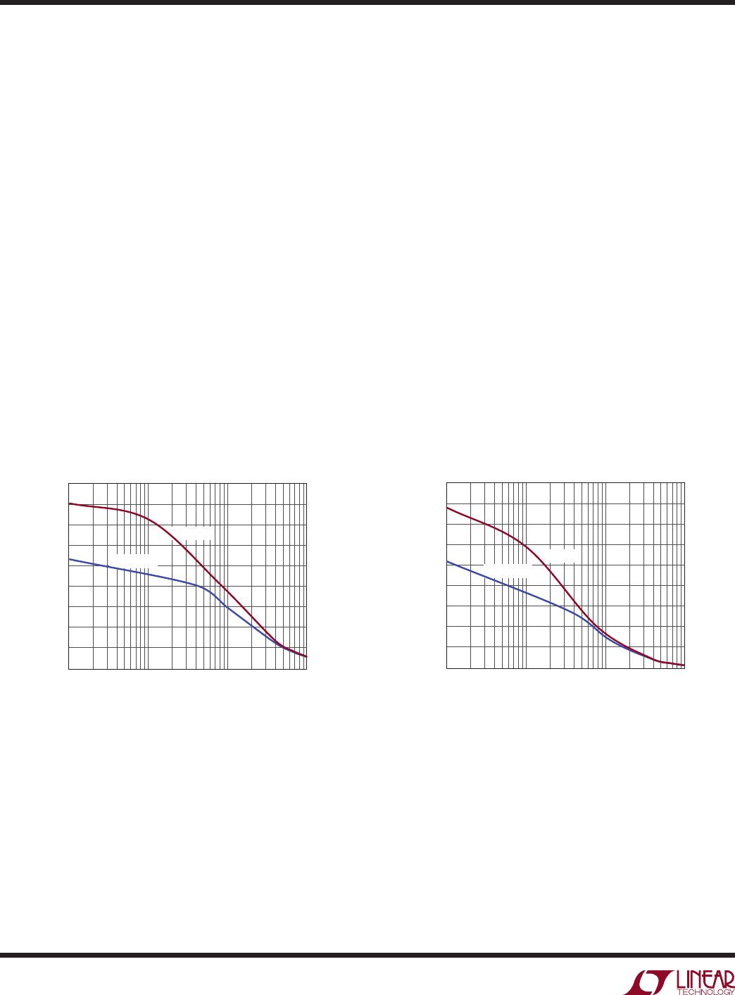
rate. For bus frequencies up to 100kHz, choose the
LTC4310-1 and refer to Figure 2 for the maximum pull-up
resistance to use. For bus frequencies between 100kHz
and 400kHz, choose the LTC4310-2 and refer to Figure 3
for the maximum pull-up resistance to use. Be sure to
include worst-case resistor tolerance when selecting
resistor value.
applicaTions inForMaTion
Rise Time Accelerators
The LTC4310’s rise time accelerator circuitry on the SDA
and SCL lines turns on during rising edges to reduce the
bus rise time. When the bus has risen above 0.45 V
CC
, the
LTC4310 turns on a strong, slew-limited pull-up current,
I
BOOST
, to help even heavily loaded buses meet the rise time
specifications. See the Typical Performance Characteristics
section for the rise time accelerator pull-up current as a
function of temperature and bus capacitance. When either
the bus has risen above (V
CC
– 1V) or 300ns after the
pull-up current has turned on (whichever comes first), the
LTC4310 deactivates its pull-up current to deter fighting
with the subsequent falling edge. Users must ensure that the
bus pull-up supply voltage V
BUS
≥ V
CC
, so that the accelera-
tors do not overdrive the SDA, SCL bus and source current
into V
BUS
. The rise time accelerators are deactivated during
start-up, thermal shutdown, shutdown and after disconnec-
tion due to a stuck bus or failure to receive a transmission
within 4.6ms.
Figure 2. Maximum SDA,SCL Bus Pull-Up Resistor Value as a
Function of Parasitic Bus Capacitance for the LTC4310-1
Figure 3. Maximum SDA,SCL Bus Pull-Up Resistor Value as
a Function of Parasitic Bus Capacitance for the LTC4310-2
C
BUS(MAX)
(pF)
1
R
BUS(MAX)
(kΩ)
10 100 1000
431012 F02
V
CC
= 5V
V
CC
= 3.3V
8
10
12
14
16
6
4
2
0
18
C
BUS(MAX)
(pF)
1
R
BUS(MAX)
(kΩ)
10 100 1000
431012 F03
8
10
12
14
16
6
4
2
0
18
V
CC
= 5V
V
CC
= 3.3V
LTC4310-1/LTC4310-2
11
431012fa
applicaTions inForMaTion
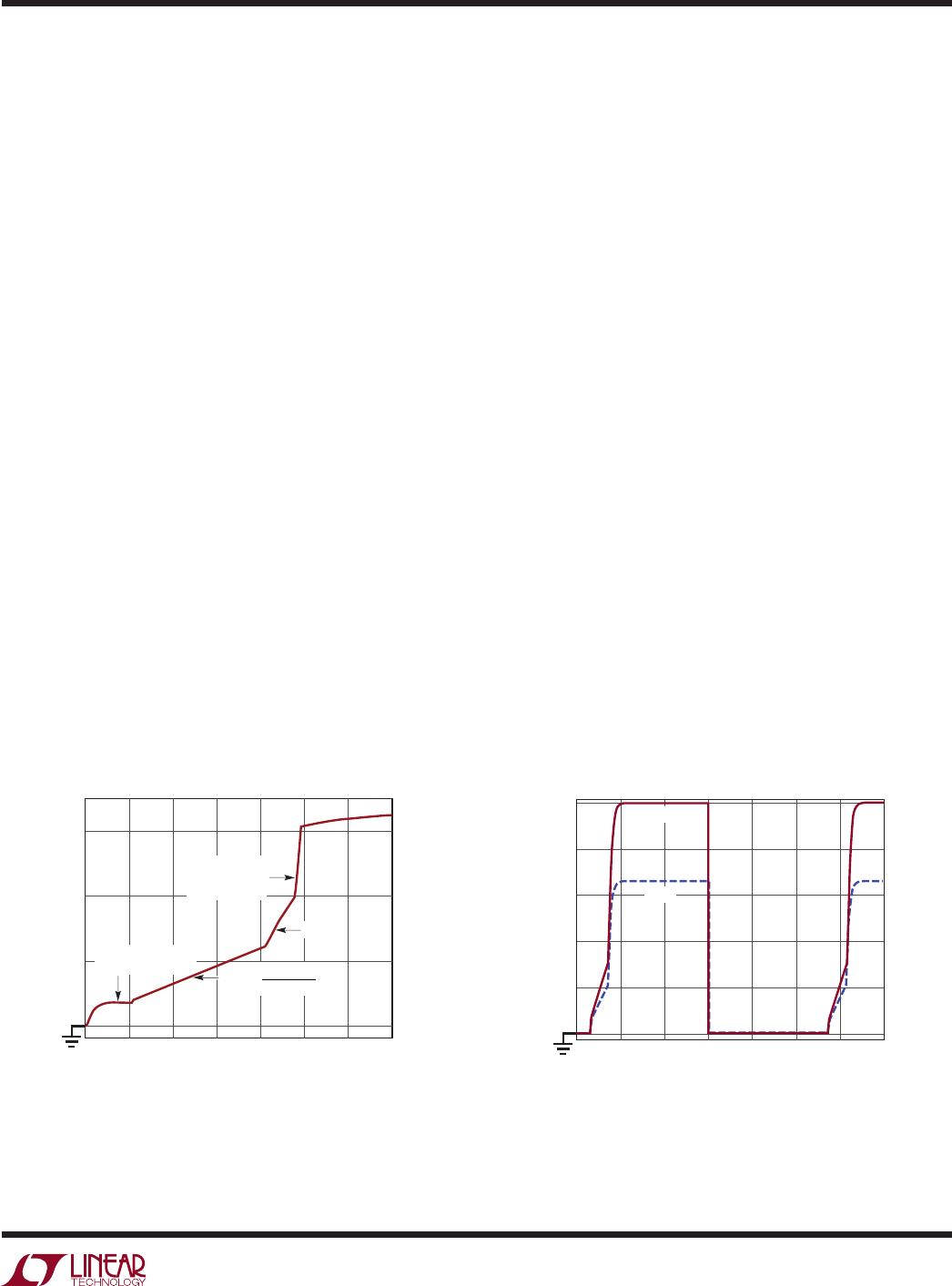
Figure 4. SCL1 Rising Waveform of SCL1
for Application Circuit Shown in Figure 1
Figure 5. 100kHz SCL Waveforms for
Application Circuit Shown in Figure 1
Bus Rising Edge Waveform
When all external pull-downs on SCL1 (Figure 1) turn off,
the SCL1 rising waveform will resemble that shown in
Figure 4. The LTC4310-1 senses that SCL1 is rising and
transmits a message to the other LTC4310-1 to release
SCL2 high. During the transmission, the first LTC4310-1
also drives SCL1 to 0.35V, so that when the transmission
is complete, both buses will rise simultaneously from
0.35V at a rate of (0.35 V
CC
)/900ns. This functionality
minimizes the effective skew between the two buses. When
SCL1 reaches 0.35 V
CC
, the LTC4310-1 deactivates its
rise rate regulation circuitry. The bus then rises with a
time constant of (R
BUS
C
BUS
) until it reaches 0.45 V
CC
,
at which point the I
BOOST
rise time accelerator pull-up
current is activated.
Figure 5 shows SCL1 and SCL2 for an entire 100kHz
switching cycle. Because the LTC4310-1 regulates the bus
rise rate to (0.35 V
CC
)/900ns, the 5V bus signal rises
more quickly than the 3.3V bus signal. Both buses reach
(0.35 V
CC
) in approximately 900ns, so the effective skew
between the buses is nearly zero. The LTC4310-2 functions
the same as the LTC4310-1, except the controlled rise rate
is limited to (0.35 • V
CC
)/300ns.
1V/DIV
200ns/DIV
BUS RC
431012 F04
SCL1 SET TO 0.35V
DURING TX
RISE TIME
ACCELERATOR
ACTIVE
0.35 • V
CC
900 ns
dV/dt =
1V/DIV
2µs/DIV
SCL1
SCL2
431012 F05
Start-Up, Data and Clock Hot Swap Circuitry
The LTC4310 contains power-on reset (POR) circuitry that
sets the data and clock pins in a high impedance state and
deactivates the transmit circuitry until the EN voltage is
high, the device is not in thermal shutdown and the V
CC
voltage is above 2.4V. After the LTC4310 exits the POR
state, it activates its transmit circuitry and communicates
its SDA, SCL logic states across the barrier to the other
LTC4310 via its TXP and TXN pins.
The receive circuitry remains deactivated for an additional
900µs after the LTC4310 exits POR. The 900µs filter time is
required for the LTC4310 to charge its RXP and RXN pins
to their DC bias voltage, assuming a 0.01µF common-mode
noise filtering capacitor at the center-tap of the secondary
side of the external transformer. When the filter time has
elapsed, the LTC4310 activates its receive circuitry and
decodes the messages it receives on its RXP and RXN
pins, registering the logic state of the remote I
2
C bus.
When both the local and remote two-wire buses are “quiet”
(i.e., no data transactions are occurring on either bus), the
LTC4310 then drives its READY pin low to indicate that it
has linked the logic state of the local I
2
C bus with the logic
state of the remote I
2
C bus. This means that the LTC4310
will now drive its SDA and SCL pins to the logic state of the
remote I
2
C bus, as specified by the messages it receives
on RXP and RXN. The LTC4310 considers a two-wire bus
LTC4310-1/LTC4310-2
12
431012fa
applicaTions inForMaTion
quiet if it has been idle high for at least 115µs, or if a STOP
bit has occurred and both data and clock have remained
high since the STOP bit. This functionality makes the
LTC4310 ideal for hot-swapping cards into and out of a
live I
2
C system. The threshold voltages for the STOP bit
and bus idle comparators are 0.5 • V
CC
.
Stuck Bus Disconnect and Recovery
An internal timer runs whenever SDA, SCL or both are low.
The timer is only reset when both SDA and SCL are high. If
the timer does not reset within 37ms, the LTC4310 assumes
the bus is stuck low. Accordingly, it ceases driving its SDA
and SCL pins and transmits a special message across the
barrier to inform the other LTC4310. Upon receiving this
message, the other LTC4310 also ceases driving its SDA
and SCL pins. At least 40µs after determining the bus
is stuck low, the LTC4310 generates up to sixteen clock
cycles on SCL in an attempt to make the slave release
the SDA line. The LTC4310 stops issuing clocks when the
SDA line releases high, or after sixteen cycles, whichever
comes first. Once the clock pulses have completed, the
LTC4310 issues a STOP bit on SDA and SCL to reset all
devices on the bus.
The LTC4310 reactivates its amplifiers and rise time ac-
celerators when the bus releases high and a STOP bit or
bus idle occurs on both the local and isolated buses, as
previously described in the Start-Up, Data and Clock Hot
Swap Circuitry section. The stuck bus disconnect and re-
covery circuitry is disabled when the LTC4310 is in UVLO,
thermal shutdown and low current shutdown.
Transmit and Receive Circuitry
Transmissions occur on the TXP and TXN pins whenever
the externally driven SDA or SCL logic state changes – in
other words, transmissions are event driven. In addition,
if SDA and SCL do not change state for 1.15ms, the
LTC4310 retransmits the logic state. The TXP and TXN pins
are driven in a pseudo differential fashion. Both pins are
driven to ground when inactive and are driven to 1.25V
(typical) in matched sets of alternating 35ns pulses to send
information across the barrier to the other LTC4310.
The LTC4310 receives and decodes the pulses sent by the
other LTC4310 on its RXP and RXN pins. Assuming the
start-up sequence previously described has been com-
pleted, the LTC4310 drives its SDA and SCL lines to the
logic state dictated by the decoded RXP and RXN signals.
The LTC4310 rejects RXP and RXN signals having less
than 500mV magnitude to provide noise immunity against
common-mode transients.The parasitic capacitances of the
LTC4310’s RXP and RXN pins and their associated board
traces form a capacitive divider with the transmit/receive
coupling capacitors, as shown in Figure 6. To guarantee
robust communications, minimize the parasitic capacitance
CPAR by minimizing the trace length from the coupling
capacitors to the RXP and RXN pins and choose coupling
capacitor values, CRXP and CRXN, that are at least ten
times larger than CPAR.
Figure 6. Parasitic Trace and Pin Capacitances
Form a Capacitive Divider with C
RXP
and C
RXN
.
Ensure C
RXP
, C
RXN
≥ 10 • C
PAR
431012 F06
CRXP
≥47pF
CRXN
≥47pF
GND
RXP
RXN
LTC4310
CPAR1
4.7pF
CPAR2
4.7pF
If the LTC4310 has not received a message in 4.6ms, it
assumes there is a communication problem and ceases
driving its SDA and SCL pins. It also transmits a special
message to the other LTC4310 to inform it that it is no
longer driving its SDA and SCL bus. Upon receiving this
message, the other LTC4310 also ceases driving its SDA and
SCL pins. Once the communication problem is resolved,
both LTC4310’s reactivate their amplifiers and rise time
accelerators after a STOP bit or bus idle has occurred on
both buses, as previously described in the Start-Up, Data
and Clock Hot Swap Circuitry section.
Thermal Shutdown
If the die temperature of the LTC4310 exceeds 150°C, the
LTC4310 enters a thermal shutdown mode. It sets TXP
and TXN to a high impedance state, ceases driving SDA
and SCL, and ignores the signals on RXP and RXN. When
the temperature drops back below 130°C, the LTC4310
goes through the POR sequence previously described.
LTC4310IMS-1#TRPBF

Mfr. #:
Manufacturer:
Analog Devices Inc.
Description:
Digital Isolators I2C Isolater, 100kHz Max Bus Frequency
Lifecycle:
New from this manufacturer.
Delivery:
DHL FedEx Ups TNT EMS
Payment:
T/T Paypal Visa MoneyGram Western Union