Copyright © Cirrus Logic, Inc. 2007
(All Rights Reserved)
http://www.cirrus.com
CS3301
Low-noise, Programmable Gain, Differential Amplifier
Features & Desription
z Signal Bandwidth: DC to 2 kHz
z Selectable Gain: x1, x2, x4, x8, x16, x32, x64
z Differential Inputs, Differential Outputs
Multiplexed inputs: INA, INB, 800 termination
Rough / fine charge outputs for CS5371/72
Max signal amplitude: 5 V
pp
differential
Low input bias: 500 pA
z Outstanding Noise Performance
•0.20µV
p-p
between 0.1 Hz and 10 Hz
8.5 from 0.1 Hz to 2 kHz
z Low Total Harmonic Distortion
-118 dB THD typical (0.000126%)
-112 dB THD maximum (0.000251%)
z Low Power Consumption
Normal/LPWR/PWDN: 5.5 mA, 3.5 mA, 10 µA
z Single or Dual Power Supply Configurations
VA+ = +5 V; VA- = 0 V; VD = +3.3 V to +5 V
VA+ = +2.5 V;VA- = -2.5 V;VD = +3.3 V
Description
The CS3301 is a low-noise differential input, differential
output amplifier with programmable gain, optimized for
amplifying signals from low-impedance sensors such as
geophones. The gain settings are binary weighted (x1,
x2, x4, x8, x16, x32, x64) and are selected using simple
pin settings. Two sets of external inputs, INA and INB,
simplify system design as inputs from a sensor and test
DAC. An internal 800 termination can also be selected
for noise tests.
Amplifier noise performance is outstanding with a noise
density of 8.5 over the 0.1 Hz to 2 kHz band-
width. Distortion performance is also extremely good,
typically -118 dB THD. Flat noise down to 0.1 Hz and
low total harmonic distortion make this amplifier ideal for
low-frequency, low-amplitude, differential signals requir-
ing maximum dynamic range.
ORDERING INFORMATION
See page 15.
nV/ Hz
nV/ Hz
INA+
INB+
MUX0
MUX1
INB-
INA-
VA+
VA-
VD
DGND
CLK
OUTR+
OUTF+
GAIN0
GAIN1
GAIN2
OUTF-
OUTR-
LPWR PWDN
+
-
-
+
400 400
500
500
500
500
DEC ‘07
DS595F3
680
680
680
680
CS3301
2 DS595F3
TABLE OF CONTENTS
1. CHARACTERISTICS AND SPECIFICATIONS .............................................................................. 4
SPECIFIED OPERATING CONDITIONS ....................................................................................... 4
ABSOLUTE MAXIMUM RATINGS ................................................................................................. 4
THERMAL CHARACTERISTICS .................................................................................................. 5
ANALOG CHARACTERISTICS ..................................................................................................... 5
DIGITAL CHARACTERISTICS ...................................................................................................... 8
POWER SUPPLY CHARACTERISTICS ........................................................................................ 9
2. GENERAL DESCRIPTION ...........................................................................................................10
2.1.Analog Signals........................................................................................................................ 10
2.2.1. Analog Inputs..............................................................................................................10
2.3.2. Analog Outputs...........................................................................................................10
2.4.3. Differential Signals......................................................................................................11
2.5.Digital Signals......................................................................................................................... 11
2.6.1. Clock Input..................................................................................................................11
2.7.2. Gain Selection ............................................................................................................11
2.8.3. Mux Selection .............................................................................................................11
2.9.4. Low Power Selection .................................................................................................. 11
2.10.5. Power Down Selection................................................................................................ 11
2.11.Power Supplies ..................................................................................................................... 11
2.12.1. Analog Power Supplies............................................................................................... 11
2.13.2. Digital Power Supplies................................................................................................ 12
2.14.Connection Diagram.............................................................................................................. 13
3. PIN DESCRIPTION .......................................................................................................................14
4. ORDERING INFORMATION ........................................................................................................15
5. ENVIRONMENTAL, MANUFACTURING, & HANDLING INFORMATION .................................. 15
6. PACKAGE DIMENSIONS............................................................................................................. 16
CS3301
DS595F3 3
LIST OF FIGURES
Figure 1. CS3301 Noise Performance ............................................................................................ 5
Figure 2. Digital Input Rise and Fall Times .....................................................................................8
Figure 3. Multi-Channel System Architecture................................................................................ 10
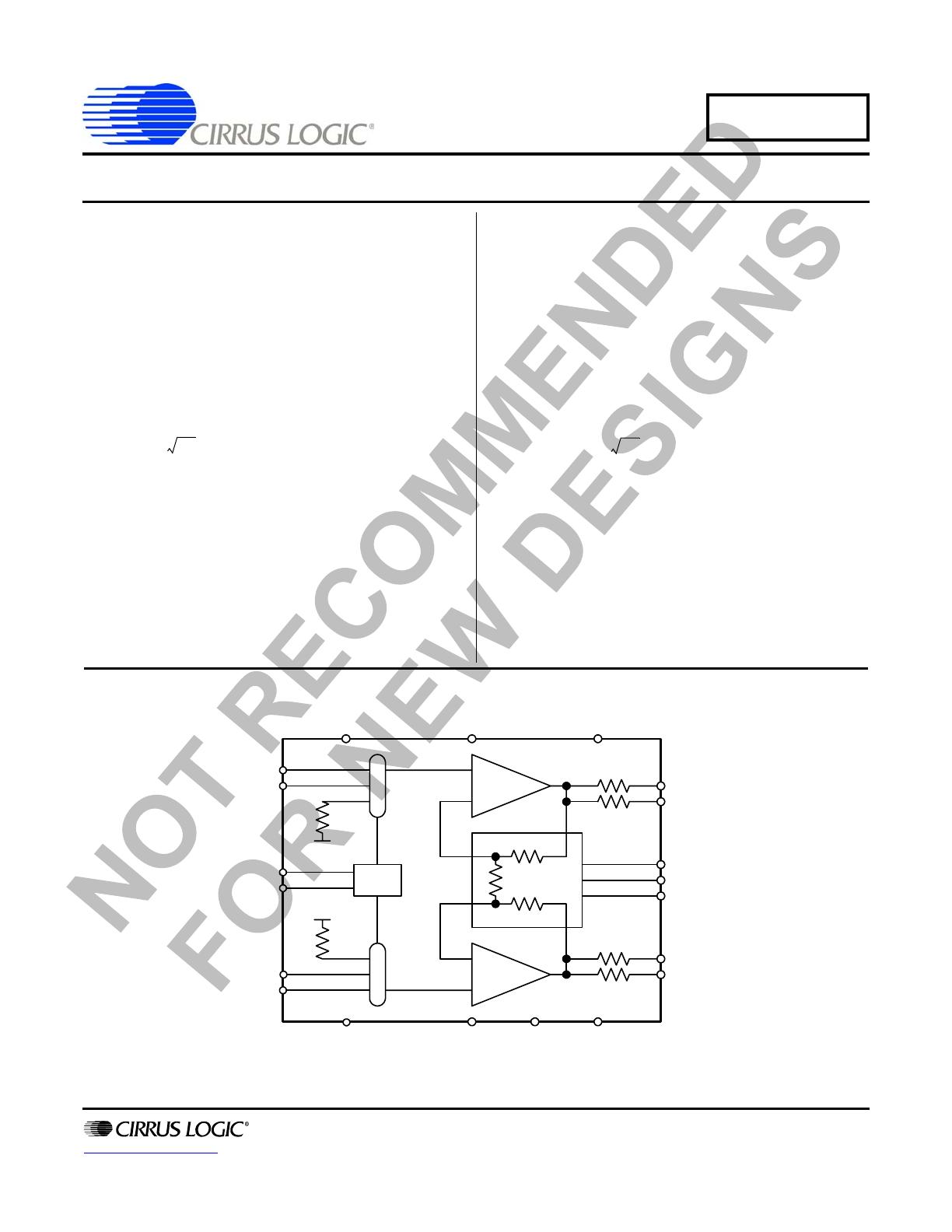
Figure 4. CS3301 Amplifier Connections...................................................................................... 13
Figure 5. CS3301 Pin Assignments .............................................................................................. 14
LIST OF TABLES
Table 1. Digital Selections for Gain and Input Mux Control ........................................................... 8
Table 2. Pin Descriptions ............................................................................................................. 14
REVISION HISTORY
Revision Date Changes
PP2 JUL 2003 Final preliminary release.
F1 AUG 2005 Updated legal notice. Added MSL data.
F2 SEP 2005 Updated anti-alias resistor values, relative gain accuracy, CS4373A part num-
ber.
F3 DEC 2007 Added watermark to indicate device is not recommended for new designs.
Contacting Cirrus Logic Support
For all product questions and inquiries contact a Cirrus Logic Sales Representative.
To find one nearest you go to www.cirrus.com
IMPORTANT NOTICE
Cirrus Logic, Inc. and its subsidiaries (“Cirrus”) believe that the information contained in this document is accurate and reliable. However, the information is subject
to change without notice and is provided “AS IS” without warranty of any kind (express or implied). Customers are advised to obtain the latest version of relevant
information to verify, before placing orders, that information being relied on is current and complete. All products are sold subject to the terms and conditions of sale
supplied at the time of order acknowledgment, including those pertaining to warranty, indemnification, and limitation of liability. No responsibility is assumed by Cirrus
for the use of this information, including use of this information as the basis for manufacture or sale of any items, or for infringement of patents or other rights of third
parties. This document is the property of Cirrus and by furnishing this information, Cirrus grants no license, express or implied under any patents, mask work rights,
copyrights, trademarks, trade secrets or other intellectual property rights. Cirrus owns the copyrights associated with the information contained herein and gives con-
sent for copies to be made of the information only for use within your organization with respect to Cirrus integrated circuits or other products of Cirrus. This consent
does not extend to other copying such as copying for general distribution, advertising or promotional purposes, or for creating any work for resale.
CERTAIN APPLICATIONS USING SEMICONDUCTOR PRODUCTS MAY INVOLVE POTENTIAL RISKS OF DEATH, PERSONAL INJURY, OR SEVERE PROP-
ERTY OR ENVIRONMENTAL DAMAGE (“CRITICAL APPLICATIONS”). CIRRUS PRODUCTS ARE NOT DESIGNED, AUTHORIZED OR WARRANTED FOR USE
IN PRODUCTS SURGICALLY IMPLANTED INTO THE BODY, AUTOMOTIVE SAFETY OR SECURITY DEVICES, LIFE SUPPORT PRODUCTS OR OTHER CRIT-
ICAL APPLICATIONS. INCLUSION OF CIRRUS PRODUCTS IN SUCH APPLICATIONS IS UNDERSTOOD TO BE FULLY AT THE CUSTOMER'S RISK AND CIR-
RUS DISCLAIMS AND MAKES NO WARRANTY, EXPRESS, STATUTORY OR IMPLIED, INCLUDING THE IMPLIED WARRANTIES OF MERCHANTABILITY AND
FITNESS FOR PARTICULAR PURPOSE, WITH REGARD TO ANY CIRRUS PRODUCT THAT IS USED IN SUCH A MANNER. IF THE CUSTOMER OR CUS-
TOMER'S CUSTOMER USES OR PERMITS THE USE OF CIRRUS PRODUCTS IN CRITICAL APPLICATIONS, CUSTOMER AGREES, BY SUCH USE, TO FULLY
INDEMNIFY CIRRUS, ITS OFFICERS, DIRECTORS, EMPLOYEES, DISTRIBUTORS AND OTHER AGENTS FROM ANY AND ALL LIABILITY, INCLUDING AT-
TORNEYS' FEES AND COSTS, THAT MAY RESULT FROM OR ARISE IN CONNECTION WITH THESE USES.
Cirrus Logic, Cirrus, and the Cirrus Logic logo designs are trademarks of Cirrus Logic, Inc. All other brand and product names in this document may be trademarks
or service marks of their respective owners.

CS3301-ISZ

Mfr. #:
Manufacturer:
Cirrus Logic
Description:
Differential Amplifiers IC Geophone Lw Noise Prgmbl Gn Dfif Amp
Lifecycle:
New from this manufacturer.
Delivery:
DHL FedEx Ups TNT EMS
Payment:
T/T Paypal Visa MoneyGram Western Union

Products related to this Datasheet