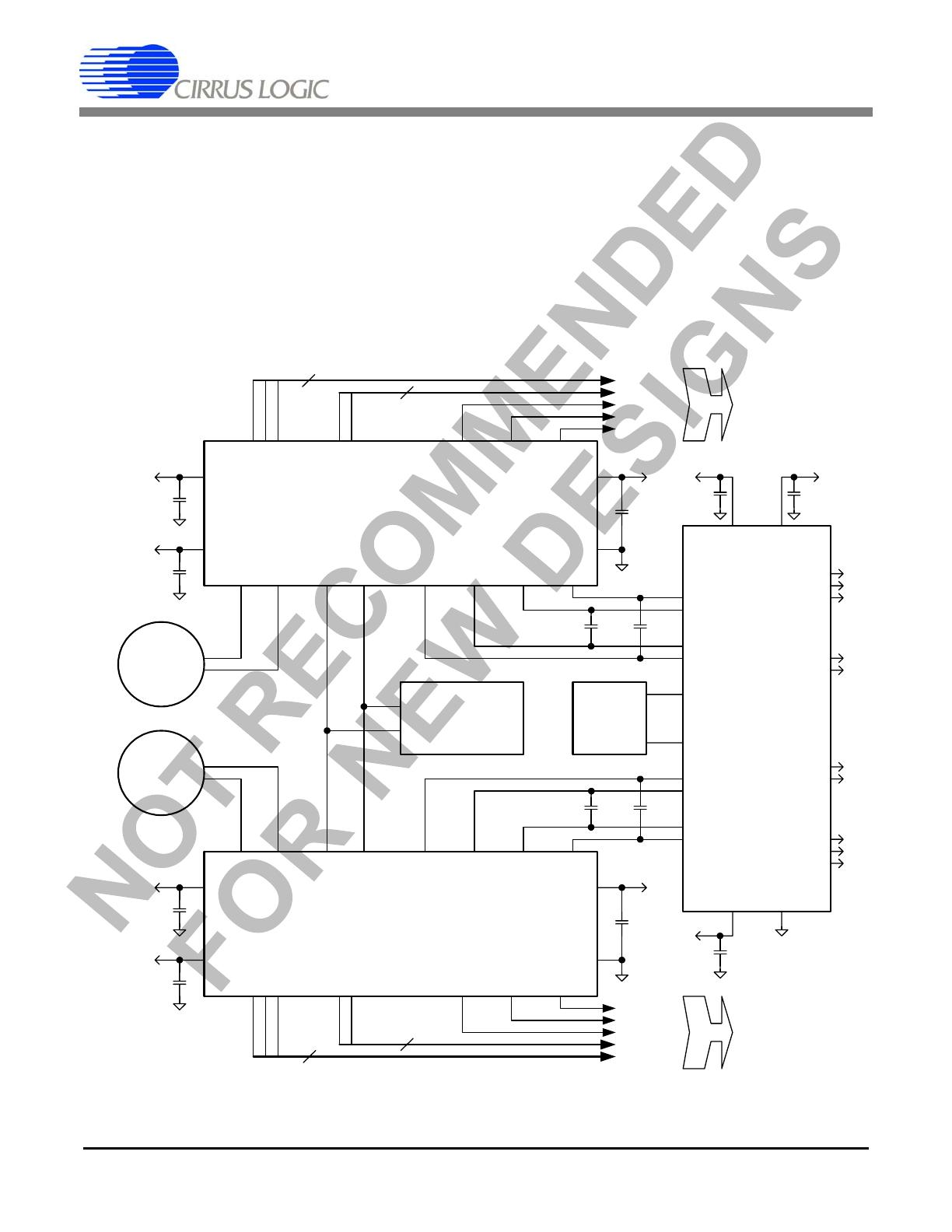
CS3301
14 DS595F3
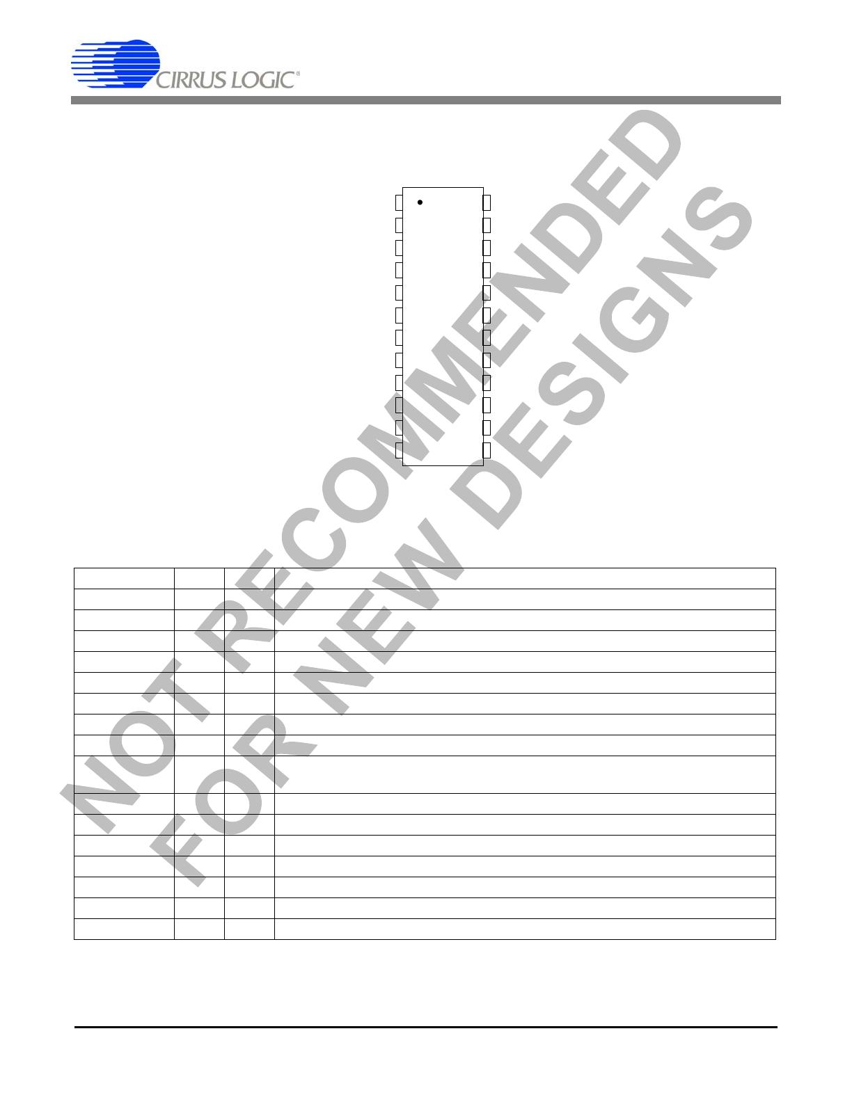
3. PIN DESCRIPTION
Pin Name Pin # I/O
Pin Description
VA+
1 I Positive analog supply voltage.
VA-
4 I Negative analog supply voltage.
VD
16 I Positive digital supply voltage.
DGND
15 I Digital ground.
INA+, INA-
5, 6 I Channel A differential analog inputs. Selected via MUX pins.
INB+, INB-
8, 7 I Channel B differential analog inputs. Selected via MUX pins.
OUTR+, OUTR-
11, 2 O Rough charge differential analog outputs.
OUTF+, OUTF-
10, 3 O Fine charge differential analog outputs.
GAIN0, GAIN1,
GAIN2
22, 21,
20
I Gain range select. See Gain Selection table in Digital Characteristics section.
CLK
13 I Master clock input. Connect to DGND to use internal oscillator.
LPWR
18 I Low power mode enable. Active high.
PWDN
19 I Power down mode enable. Active high.
MUX0, MUX1
24, 23 I Analog input select. See Input Selection table in Digital Characteristics section.
TEST0
12 I Test mode select, factory use only. Connect to VA- during normal operation.
TEST1, TEST2
17, 14 I
Test mode select, factory use only. Connect to DGND during normal operation.
TESTOUT
9O
Test mode output, factory use only. Connect to VA- during normal operation.
Table 2. Pin Descriptions
1
2
3
4
5
6
7
817
18
19
20
21
22
23
24
9
10
11
12 13
14
15
16
Positive Analog Power Supply VA+
Negative Analog Rough Output OUTR-
Negative Analog Fine Output OUTF-
Negative Analog Power Supply VA-
Non-Inverting Input A INA+
Inverting Input A INA-
Inverting Input B INB-
Non-Inverting Input B INB+
Test Mode Output TESTOUT
Positive Analog Fine Output OUTF+
Positive Analog Rough Output OUTR+
Test Mode Select TEST0
MUX0 Input Mux Select
MUX1 Input Mux Select
GAIN0 Gain Range Select
GAIN1 Gain Range Select
GAIN2 Gain Range Select
PWDN Power Down Mode Enable
LPWR Low Power Mode Enable
TEST1 Test Mode Select
VD Positive Digital Power Supply
DGND Digital Ground
TEST2 Test Mode Select
CLK Clock Input
Figure 5. CS3301 Pin Assignments