CS3301
4 DS595F3
1. CHARACTERISTICS AND SPECIFICATIONS
Min/Max characteristics and specifications are guaranteed over the Specified Operating Conditions.
Typical performance characteristics and specifications are derived from measurements taken at nom-
inal supply voltages and T
A
= 25°C.
DGND = 0 V, all voltages with respect to 0 V.
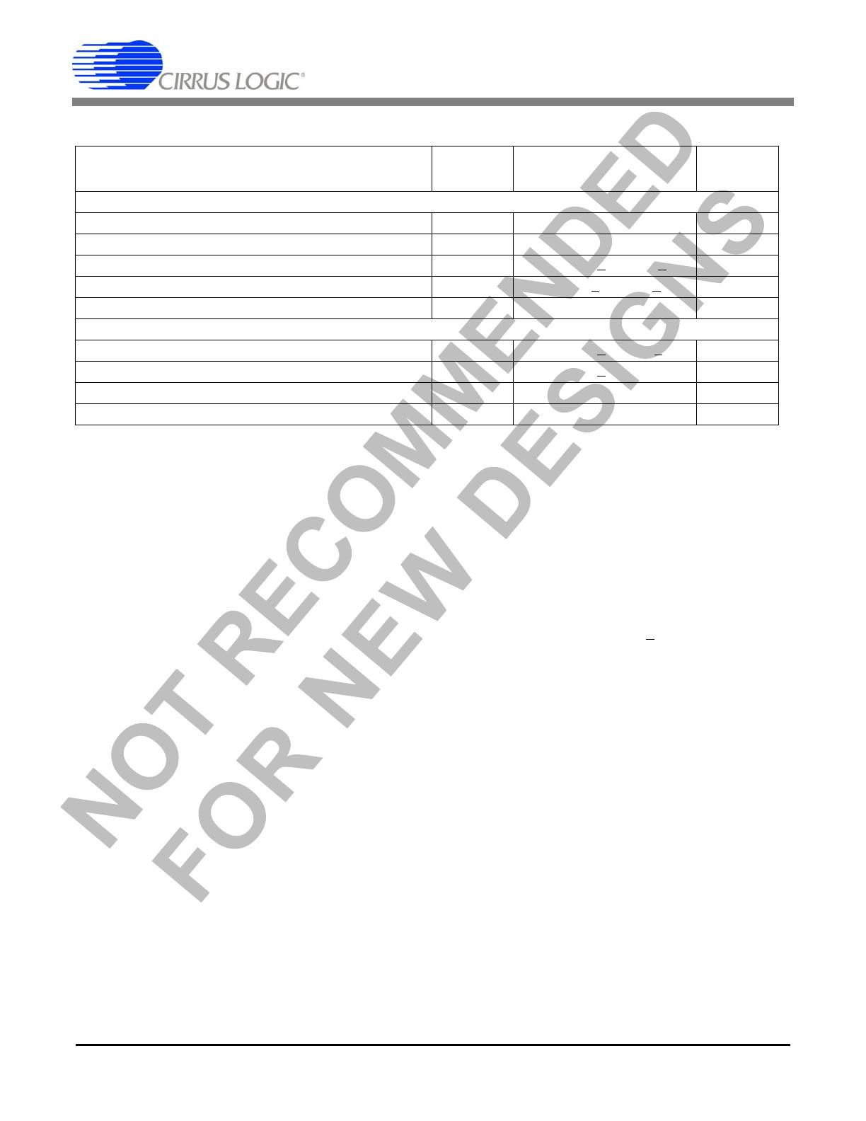
SPECIFIED OPERATING CONDITIONS
Notes: 1. VA- must be the most negative voltage to avoid potential SCR latch-up conditions.
2. VD must conform to Digital Supply Differential under Absolute Maximum Ratings.
ABSOLUTE MAXIMUM RATINGS
WARNING: Operation at or beyond these limits may result in permanent damage to the device.
Normal operation is not guaranteed at these extremes.
Notes: 3. Transient currents up to 100 mA will not cause SCR latch-up.
Parameter Symbol Min Nom Max Unit
Unipolar Power Supplies
Positive Analog VA+ 4.75 5.0 5.25 V
Negative Analog (Note 1) VA- -0.25 0 0.25 V
Positive Digital (Note 2) VD 3.135 3.3 5.25 V
Bipolar Power Supplies
Positive Analog VA+ 2.375 2.5 2.625 V
Negative Analog (Note 1) VA- -2.625 -2.5 -2.375 V
Positive Digital (Note 2) VD 3.135 3.3 3.465 V
Thermal
Ambient Operating Temperature Industrial (-IS) T
A
-40 - 85 °C
Parameter Symbol Min Max Parameter
DC Power Supplies Positive Analog
Negative Analog
Digital
VA+
VA-
VD
-0.3
-6.8
-0.3
6.8
0.3
6.8
V
V
V
Analog Supply Differential [(VA+) - (VA-)] VA
DIFF
-6.8V
Digital Supply Differential [(VD) - (VA-)] VD
DIFF
-6.8V
Input Current, Any Pin Except Supplies (Note 3)I
IN
-+10 mA
Input Current, Power Supplies (Note 3)I
IN
-+50 mA
Output Current (Note 3)I
OUT
-+25 mA
Power Dissipation PDN - 500 mW
Analog Input Voltages V
INA
(VA-)-0.5 (VA+)+0.5 V
Digital Input Voltages V
IND
-0.5 (VD)+0.5 V
Ambient Operating Temperature (Power Applied) T
A
-40 85 ºC
Storage Temperature Range T
STG
-65 150 ºC
CS3301
DS595F3 5
THERMAL CHARACTERISTICS
ANALOG CHARACTERISTICS
Notes: 4. Guaranteed by design and/or characterization.
5. Tested with a full scale input signal of 31.25 Hz.
6. Noise in the harmonic bins dominates THD and linearity measurements for x16, x32, x64 gains.
Parameter Symbol Min Typ Max Unit
Allowable Junction Temperature - - 135 ºC
Junction to Ambient Thermal Impedance Θ
JA
-
65
-
ºC / W
Ambient Operating Temperature (Power Applied) T
A
-40 - +85 ºC
Parameter Symbol
CS3301
UnitMin Typ Max
Noise Performance, Normal
Input Voltage Noise f
0
= 0.1 Hz to 10 Hz VN
PP
- 0.20 0.40 µV
p-p
Input Voltage Noise Density f
0
= 0.1 Hz to 2 kHz VN
D
-8.512.0
Input Current Noise Density (Note 4)IN
D
-200-
Noise Performance, Low Power (LPWR=1)
Input Voltage Noise f
0
= 0.1 Hz to 10 Hz VN
PP
- 0.25 0.50 µV
p-p
Input Voltage Noise Density f
0
= 0.1 Hz to 2 kHz VN
D
- 10.0 15.0
Input Current Noise Density (Note 4)IN
D
-100-
Distortion Performance, Normal
Total Harmonic Distortion (Note 5, 6) THD - -118 -112 dB
Linearity (Note 5, 6)LIN -
0.000126 0.000251
%
Distortion Performance, Low Power (LPWR=1)
Total Harmonic Distortion (Note 5, 6) THD - -118 -110 dB
Linearity (Note 5, 6)LIN -
0.000126 0.000316
%
nV/ Hz
fA/ Hz
nV/ Hz
fA/ Hz
CS3301 In-Band Noise
0
5
10
15
20
0 200 400 600 800 1000 1200 1400 1600 1800 2000
Frequency (Hz)
Noise Density (nV/rtHz)
CS3301 Wide Band Noise
0
50
100
150
200
250
300
0.1 1 10 100 1000 10000 100000 1E+06
Frequency (Hz)
Noise Density (nV/rtHz)
Figure 1. CS3301 Noise Performance
CS3301
6 DS595F3
ANALOG CHARACTERISTICS (CONT.)
7. Common mode signals pass through the differential amplifier architecture.
8. Absolute gain accuracy tests the matching of x1 gain across multiple CS3301 devices.
9. Relative gain accuracy tests the tracking of x1,x2,x4,x16,x32,x64 gain relative to x8 gain on a single
CS3301 device.
10. Specification is for the parameter over the specified temperature range and is for the CS3301 device
only. It does not include the effects of external components.
11. Offset voltage is tested with the amplifier inputs connected to the internal 800 termination.
12. The absolute offset after calibration specification applies to the effective offset voltage of the CS3301
output when used with the CS5371/72 modulator and CS5376A digital filter, and is measured from the
digitally calibrated output codes of the CS5376A.
13. The CS3301 offset calibration is performed digitally with the CS5371/72 modulator and CS5376A digital
filter and includes the full scale signal range. Calibration offsets of greater than +
5% of full scale will
begin to subtract from system dynamic range.
Parameter Symbol
CS3301
UnitMin Typ Max
Gain
Gain, Differential GAIN x1 - x64
Gain, Common Mode (Note 7)GAIN
CM
-x1-
Gain Accuracy, Absolute (Note 8)GAIN
ABS
-+1+2%
Gain Accuracy, Relative (Note 9)GAIN
REL
-+0.2 +0.5 %
Gain Drift (Note 4, 10)GAIN
TC
-5-ppm/ºC
Offset
Offset Voltage, Input Referred (Note 11)OFST - +
5+15 µV
Offset After Calibration, Absolute (Note 12)OFST
CAL
-+1- µV
Offset Calibration Range (Note 13)OFST
RNG
-100-% F.S.
Offset Voltage Drift (Note 4, 10)OFST
TC
-0.1-µV/ºC

CS3301-ISZ

Mfr. #:
Manufacturer:
Cirrus Logic
Description:
Differential Amplifiers IC Geophone Lw Noise Prgmbl Gn Dfif Amp
Lifecycle:
New from this manufacturer.
Delivery:
DHL FedEx Ups TNT EMS
Payment:
T/T Paypal Visa MoneyGram Western Union

Products related to this Datasheet