2.5 V/3.3 V, Four LVPECL Outputs,
SiGe Clock Fanout Buffer
ADCLK944
Rev. 0
Information furnished by Analog Devices is believed to be accurate and reliable. However, no
responsibility is assumed by Analog Devices for its use, nor for any infringements of patents or other
rights of third parties that may result from its use. Specifications subject to change without notice. No
license is granted by implication or otherwise under any patent or patent rights of Analog Devices.
Trademarks and registered trademarks are the property of their respective owners.
One Technology Way, P.O. Box 9106, Norwood, MA 02062-9106, U.S.A.
Tel: 781.329.4700 www.analog.com
Fax: 781.461.3113 ©2010 Analog Devices, Inc. All rights reserved.
FEATURES FEATURES
Operating frequency: 7.0 GHz Operating frequency: 7.0 GHz
Broadband random jitter: 50 fs rms Broadband random jitter: 50 fs rms
On-chip input terminations On-chip input terminations
Power supply (V
CC
V
EE
): 2.5 V to 3.3 V Power supply (V
CC
V
EE
): 2.5 V to 3.3 V
APPLICATIONS APPLICATIONS
Low jitter clock distribution Low jitter clock distribution
Clock and data signal restoration Clock and data signal restoration
Level translation Level translation
Wireless communications Wireless communications
Wired communications Wired communications
Medical and industrial imaging Medical and industrial imaging
ATE and high performance instrumentation ATE and high performance instrumentation
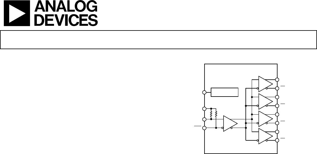
FUNCTIONAL BLOCK DIAGRAM FUNCTIONAL BLOCK DIAGRAM
LVPECL
ADCLK944
REFERENCE
REF
V
T
Q0
Q0
Q1
Q1
Q2
V
CLK
Q2
Q3
Q3
CLK
0
8770-001
Figure 1.
GENERAL DESCRIPTION
The ADCLK944 is an ultrafast clock fanout buffer fabricated on
the Analog Devices, Inc., proprietary XFCB3 silicon germanium
(SiGe) bipolar process. This device is designed for high speed
applications requiring low jitter.
The device has a differential input equipped with center-tapped,
differential, 100 Ω on-chip termination resistors. The input can
accept dc-coupled LVPECL, CML, 3.3 V CMOS (single-ended),
and ac-coupled 1.8 V CMOS, LVDS, and LVPECL inputs. A V
REF
pin is available for biasing ac-coupled inputs.
The ADCLK944 features four full-swing emitter-coupled logic
(ECL) output drivers. For LVPECL (positive ECL) operation,
bias V
CC
to the positive supply and V
EE
to ground. For ECL
operation, bias V
CC
to ground and V
EE
to the negative supply.
The ECL output stages are designed to directly drive 800 mV
each side into 50 Ω terminated to V
CC
− 2 V for a total differen-
tial output swing of 1.6 V.
The ADCLK944 is available in a 16-lead LFCSP and is specified
for operation over the standard industrial temperature range of
−40°C to +85°C.
ADCLK944* PRODUCT PAGE QUICK LINKS
Last Content Update: 02/23/2017
COMPARABLE PARTS
View a parametric search of comparable parts.
EVALUATION KITS
ADCLK944 Evaluation Board
DOCUMENTATION
Data Sheet
ADCLK944: 2.5 V/3.3 V, Four LVPECL Outputs,SiGe Clock
Fanout Buffer
User Guides
UG-125: Setting Up the Evaluation Board for the
ADCLK944
TOOLS AND SIMULATIONS
ADIsimCLK Design and Evaluation Software
ADCLK944 IBIS Model
REFERENCE MATERIALS
Technical Articles
Design A Clock-Distribution Strategy With Confidence
Speedy A/Ds Demand Stable Clocks
Understand the Effects of Clock Jitter and Phase Noise on
Sampled Systems
Tutorials
MT-008: Converting Oscillator Phase Noise to Time Jitter
DESIGN RESOURCES
ADCLK944 Material Declaration
PCN-PDN Information
Quality And Reliability
Symbols and Footprints
DISCUSSIONS
View all ADCLK944 EngineerZone Discussions.
SAMPLE AND BUY
Visit the product page to see pricing options.
TECHNICAL SUPPORT
Submit a technical question or find your regional support
number.
DOCUMENT FEEDBACK
Submit feedback for this data sheet.
This page is dynamically generated by Analog Devices, Inc., and inserted into this data sheet. A dynamic change to the content on this page will not
trigger a change to either the revision number or the content of the product data sheet. This dynamic page may be frequently modified.
ADCLK944
Rev. 0 | Page 2 of 12
TABLE OF CONTENTS
Features .............................................................................................. 1
Applications ....................................................................................... 1
Functional Block Diagram .............................................................. 1
General Description ......................................................................... 1
Revision History ............................................................................... 2
Specifications ..................................................................................... 3
Clock Inputs and Outputs ........................................................... 3
Timing Characteristics ................................................................ 3
Power .............................................................................................. 4
Absolute Maximum Ratings ............................................................ 5
Determining Junction Temperature .......................................... 5
ESD Caution...................................................................................5
Thermal Performance ...................................................................5
Pin Configuration and Function Descriptions ..............................6
Typical Performance Characteristics ..............................................7
Theory of Operation .........................................................................9
Clock Inputs ...................................................................................9
Clock Outputs ................................................................................9
PCB Layout Considerations ...................................................... 10
Input Termination Options ....................................................... 11
Outline Dimensions ....................................................................... 12
Ordering Guide .......................................................................... 12
REVISION HISTORY
3/10—Revision 0: Initial Version

ADCLK944BCPZ-R7

Mfr. #:
Manufacturer:
Analog Devices Inc.
Description:
Clock Buffer 2.5V/3.3V 4-LVPECL Outputs SiGe
Lifecycle:
New from this manufacturer.
Delivery:
DHL FedEx Ups TNT EMS
Payment:
T/T Paypal Visa MoneyGram Western Union

Products related to this Datasheet