ADCLK944
Rev. 0 | Page 9 of 12
THEORY OF OPERATION
CLOCK INPUTS
The ADCLK944 accepts a differential clock input and distrib-
utes it to all four LVPECL outputs. The maximum specified
frequency is the point at which the output voltage swing is 50%
of the standard LVPECL swing (see Figure 4).
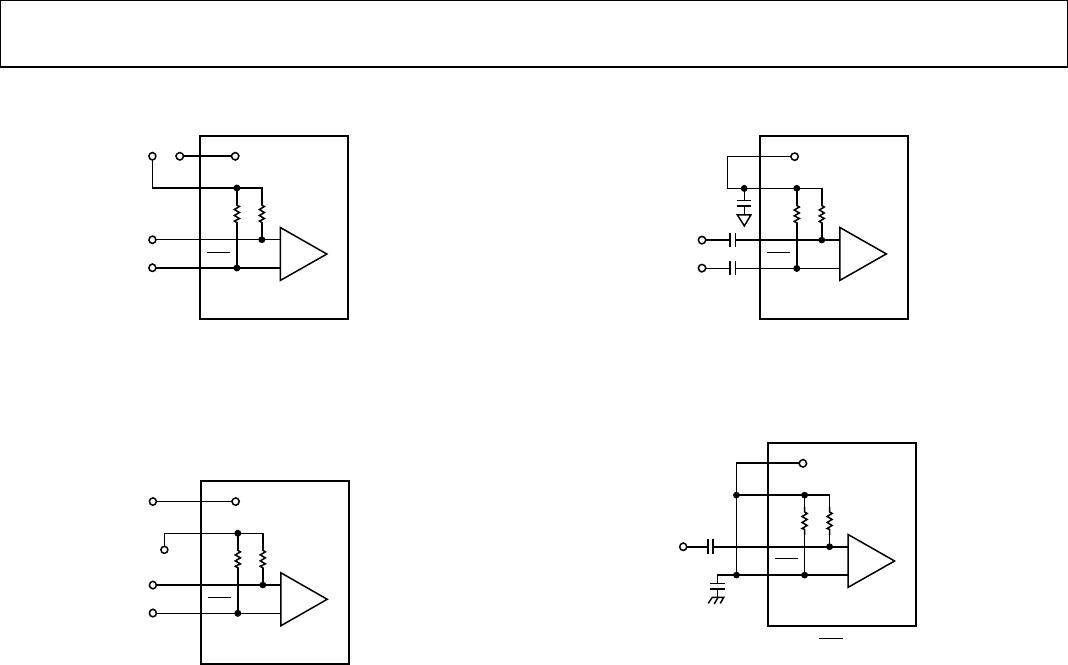
The device has a differential input equipped with center-tapped,
differential, 100 Ω on-chip termination resistors. The input can
accept dc-coupled LVPECL, CML, 3.3 V CMOS (single-ended,
3.3 V operation only), and ac-coupled 1.8 V CMOS, LVDS, and
LVPECL inputs. A V
REF
pin is available for biasing ac-coupled
inputs (see Figure 20 and Figure 21).
Maintain the differential input voltage swing from approxi-
mately 400 mV p-p to no more than 3.4 V p-p. See Figure 18
through Figure 21 for various clock input termination schemes.
Output jitter performance is significantly degraded by an input
slew rate below 1 V/ns, as shown in Figure 11. The ADCLK944
is specifically designed to minimize added random jitter over a
wide input slew rate range. Whenever possible, clamp excessively
large input signals with fast Schottky diodes because attenuators
reduce the slew rate. Input signal runs of more than a few centi-
meters should be over low loss dielectrics or cables with good
high frequency characteristics.
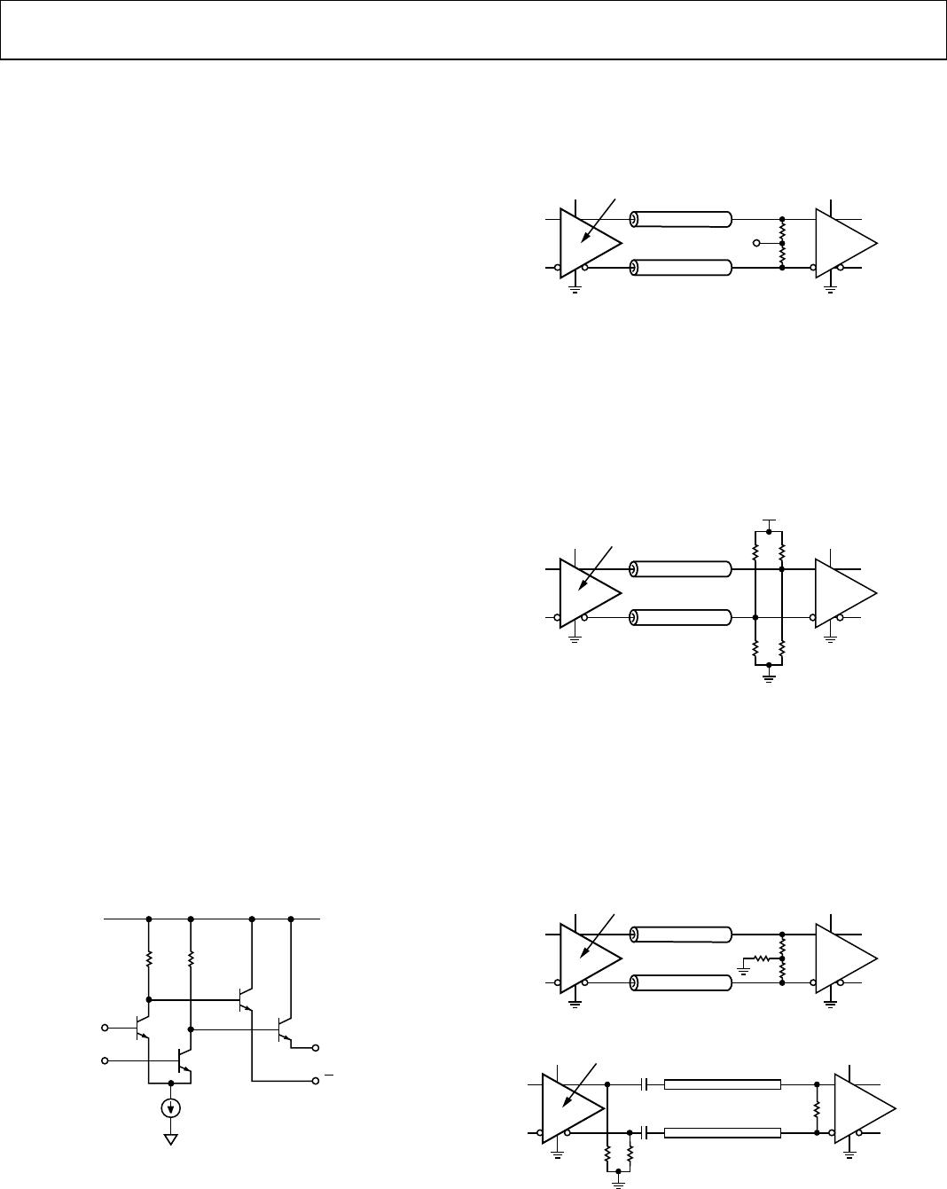
CLOCK OUTPUTS
The specified performance necessitates using proper transmis-
sion line terminations. The LVPECL outputs of the ADCLK944
are designed to directly drive 800 mV into a 50 Ω cable or into
microstrip/stripline transmission lines terminated with 50 Ω
referenced to V
CC
− 2 V, as shown in Figure 13. The LVPECL
output stage is shown in Figure 12. The outputs are designed
for best transmission line matching. If high speed signals must
be routed more than a centimeter, either the microstrip or the
stripline technique is required to ensure proper transition times
and to prevent excessive output ringing and pulse-width-dependent
propagation delay dispersion.
V
EE
V
CC
Q
Q
08770-013
Figure 12. Simplified Schematic Diagram
of the LVPECL Output Stage
Figure 13 through Figure 16 depict various LVPECL output
termination schemes. When dc-coupled, V
CC
of the receiving
buffer should match VS_DRV.
A
DCLK944
V
S_DRV
V
CC
= VS_DR
Z
0
= 50
LVPECL
50
V
CC
– 2V
50
08770-014
Z
0
= 50
Figure 13. DC-Coupled, 3.3 V LVPECL
Thevenin-equivalent termination uses a resistor network to provide
50 Ω termination to a dc voltage that is below V
OL
of the LVPECL
driver. In this case, VS_DRV on the ADCLK944 should equal
V
CC
of the receiving buffer. Although the resistor combination
shown in Figure 14 results in a dc bias point of VS_DRV − 2 V,
the actual common-mode voltage is VS_DRV − 1.3 V because
there is additional current flowing from the ADCLK944 LVPECL
driver through the pull-down resistor.
VS_DRV
50
50
SINGLE-ENDED
(NOT COUPLED)
V
S_DRV
ADCLK944
V
CC
LVPECL
127 127
83 83
8770-015
0
Figure 14. DC-Coupled, 3.3 V LVPECL Far-End Thevenin Termination
LVPECL Y-termination (see Figure 15) is an elegant termination
scheme that uses the fewest components and offers both odd-
and even-mode impedance matching. Even-mode impedance
matching is an important consideration for closely coupled trans-
mission lines at high frequencies. Its main drawback is that it offers
limited flexibility for varying the drive strength of the emitter-
follower LVPECL driver. This can be an important consideration
when driving long trace lengths but is usually not an issue.
A
DCLK944
VS_DRV V
CC
= VS_DRV
Z
0
= 50
LVPECL
50
50
50
8770-016
Z
0
= 50
0
Figure 15. DC-Coupled, 3.3 V LVPECL Y-Termination
A
VS_DRV
100 DIFFERENTIAL
(COUPLED)
TRANSMISSION LINE
V
CC
LVPECL
100
0.1nF
0.1nF
DCLK944
200 200
08770-017
Figure 16. AC-Coupled LVPECL with Parallel Transmission Line
ADCLK944
Rev. 0 | Page 10 of 12
PCB LAYOUT CONSIDERATIONS
The ADCLK944 buffer is designed for very high speed applica-
tions. Consequently, high speed design techniques must be used
to achieve the specified performance. It is critically important to
use low impedance supply planes for both the negative supply
(V
EE
) and the positive supply (V
CC
) planes as part of a multilayer
board. Providing the lowest inductance return path for switching
currents ensures the best possible performance in the target
application.
The following references to the ground plane assume that the V
EE
power plane is grounded for LVPECL operation. Note that, for
ECL operation, the V
CC
power plane becomes the ground plane.
It is also important to adequately bypass the input and output
supplies. Place a 1 µF electrolytic bypass capacitor within several
inches of each V
CC
power supply pin to the ground plane. In
addition, place multiple high quality 0.001 F bypass capacitors
as close as possible to each V
CC
supply pin, and connect the
capacitors to the ground plane with redundant vias. Select high
frequency bypass capacitors for minimum inductance and ESR.
To improve the effectiveness of the bypass at high frequencies,
minimize parasitic layout inductance. Also, avoid discontinuities
along input and output transmission lines; such discontinuities
can affect jitter performance.
In a 50 Ω environment, input and output matching have a signif-
icant impact on performance. The buffer provides internal 50 Ω
termination resistors for both the CLK and
CLK
inputs. Normally,
the return side is connected to the reference pin that is provided.
Bypass the termination potential using ceramic capacitors to
prevent undesired aberrations on the input signal due to parasitic
inductance in the termination return path. If the inputs are dc-
coupled to a source, take care to ensure that the pins are within
the rated input differential and common-mode voltage ranges.
If the return is floated, the device exhibits a 100  cross-termi-
nation, but the source must then control the common-mode
voltage and supply the input bias currents.
ESD/clamp diodes between the input pins prevent the application
from developing excessive offsets to the input transistors. ESD
diodes are not optimized for best ac performance. When a clamp
is required, it is recommended that appropriate external diodes
be used.
Exposed Metal Paddle
The exposed metal paddle on the ADCLK944 package is both an
electrical connection and a thermal enhancement. For the device
to function properly, the paddle must be properly attached to
the V
EE
pins.
When properly mounted, the ADCLK944 also dissipates heat
through its exposed paddle. The PCB acts as a heat sink for the
ADCLK944. The PCB attachment must provide a good thermal
path to a larger heat dissipation area. This requires a grid of vias
from the top layer of the PCB down to the V
EE
power plane (see
Figure 17). The ADCLK944 evaluation board (ADCLK944/PCBZ)
provides an example of how to attach the part to the PCB.
VIAS TO V
EE
POWER
PLANE
08770-018
Figure 17. PCB Land for Attaching Exposed Paddle
ADCLK944
Rev. 0 | Page 11 of 12
INPUT TERMINATION OPTIONS
V
REF
V
CC
V
T
CLK
CLK
V
REF
V
T
CONNECT V
T
TO V
CC
.
08770-019
5050
Figure 18. Interfacing to CML Inputs
V
REF
V
T
CONNECT V
T
TO V
CC
2V.
V
CC
– 2V
5050
CLK
CLK
08770-020
Figure 19. Interfacing to PECL Inputs
CONNECT V
T
TO V
REF
.
5050
CLK
CLK
08770-021
V
REF
V
T
Figure 20. AC Coupling Differential Signal Inputs, Such as LVDS
C
ONNECT V
T
, V
REF
, AND CLK TOGETHER.
PLACE A BYPASS CAPACITOR FROM V
T
TO
G
ROUND.
A
LTERNATIVELY, V
T
, V
REF
, AND CLK CAN BE
C
ONNECTED TOGETHER, GIVING A CLEANE
LAY
5050
CLK
CLK
08770-022
R
OUT AND A 180° PHASE SHIFT.
Figure 21. Interfacing to AC-Coupled, Single-Ended Inputs

ADCLK944BCPZ-R7

Mfr. #:
Manufacturer:
Analog Devices Inc.
Description:
Clock Buffer 2.5V/3.3V 4-LVPECL Outputs SiGe
Lifecycle:
New from this manufacturer.
Delivery:
DHL FedEx Ups TNT EMS
Payment:
T/T Paypal Visa MoneyGram Western Union

Products related to this Datasheet