Data Sheet ADuM4151/ADuM4152/ADuM4153
V
DD1
1
GND
1
2
MCLK
3
MO
4
20
19
18
17
MI
5
MSS
6
V
IA
7
16
15
14
V
OB
8
13
V
OC
9
12
GND
1
V
DD2
GND
2
SCLK
SI
SO
SSS
V
OA
V
IB
V
IC
GND
2
10
11
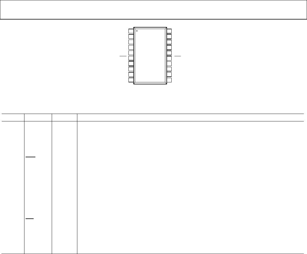
ADuM4152
TOP VIEW
(Not to Scale)
12370-006
Figure 6. ADuM4152 Pin Configuration
Table 21. ADuM4152 Pin Function Descriptions
Pin No. Mnemonic
Direction Description
1 V
DD1
Power Input Power Supply for Isolator Side 1. A bypass capacitor from V
DD1
to GND
1
to local ground is required.
2, 10 GND
1
Return Ground 1. Ground reference for Isolator Side 1.
3 MCLK
Clock SPI Clock from the Master Controller.
4 MO Input SPI Data from the Master to the Slave MO/SI Line.
5 MI Output SPI Data from the Slave to the Master MI/SO Line.
6
MSS
Input Slave Select from the Master. This signal uses an active low logic. The slave select pin requires a 10 ns
setup time from the next clock or data edge.
7 V
IA
Input Low Speed Data Input A.
8 V
OB
Output Low Speed Data Output B.
9 V
OC
Output Low Speed Data Output C.
11, 19 GND
2
Return Ground 2. Ground reference for Isolator Side 2.
12 V
IC
Input Low Speed Data Input C.
13 V
IB
Input Low Speed Data Input B.
14 V
OA
Output Low Speed Data Output A.
SSS
Slave Select to the Slave. This signal uses an active low logic.
16 SO Input SPI Data from the Slave to the Master MI/SO Line.
17 SI Output SPI Data from the Master to the Slave MO/SI Line.
18 SCLK Output SPI Clock from the Master Controller.
20 V
DD2
Power Input Power Supply for Isolator Side 2. A bypass capacitor from V
DD2
to GND
2
to local ground is required.
Rev. A | Page 15 of 22