ADuM4151/ADuM4152/ADuM4153 Data Sheet
APPLICATIONS INFORMATION
INTRODUCTION
The ADuM4151/ADuM4152/ADuM4153 are a family of devices
created to optimize isolation of SPI for speed and to provide
additional low speed channels for control and status monitoring
functions. The isolators are based on differential signaling
iCoupler technology for enhanced speed and noise immunity.
High Speed Channels
The ADuM4151/ADuM4152/ADuM4153 have four high speed
channels. The first three channels, CLK, MI/SO, and MO/SI
(the slash indicates the connection of the particular input and
output channel across the isolator), are optimized for either low
propagation delay in the B grade or high noise immunity in the
A grade. The difference between the grades is the addition of a
glitch filter to these three channels in the A grade version,
which increases the propagation delay. The B grade version,
with a maximum propagation delay of 14 ns, supports a
maximum clock rate of 17 MHz in the standard 4-wire SPI.
However, because the glitch filter is not present in the B grade
version, ensure that spurious glitches of less than 10 ns are not
present.
Glitches of less than 10 ns in the B grade devices can cause the
missing of the second edge of the glitch. This pulse condition is
then seen as a spurious data transition on the output that is
corrected by a refresh or the next valid data edge. It is recommended
to use the A grade devices in noisy environments.
The relationship between the SPI signal paths and the pin
mnemonics of the ADuM4151/ADuM4152/ADuM4153 and the
data directions is detailed in Table 24.
Table 24. Pin Mnemonics Correspondence to the SPI Signal
Path Names
SPI Signal Path Master Side 1 Data Direction Slave Side 2
CLK MCLK
SCLK
MO/SI MO
SI
MI/SO MI
SO
SS
MSS
SSS
The datapaths are SPI mode agnostic. The CLK and MO/SI SPI
datapaths are optimized for propagation delay and channel to
channel matching. The MI/SO SPI datapath is optimized for
propagation delay. The devices do not synchronize to the clock
channels; therefore, there are no constraints on the clock
polarity or the timing with respect to the data lines. To allow
compatibility with nonstandard SPI interfaces, the MI pin is
always active, and does not tristate when the slave select is not
asserted. This precludes tying several MI lines together without
adding a trisate buffer or multiplexor.
SS
(slave select bar) is typically an active low signal.
SS
can have
many different functions in SPI and SPI like busses. Many of
these functions are edge triggered; therefore, the
SS
path contains a
glitch filter in both the A grade and the B grade. The glitch filter
prevents short pulses from propagating to the output or causing
other errors in operation. The
MSS
signal requires a 10 ns setup
time in the B grade devices prior to the first active clock edge to
allow the added propagation time of the glitch filter.
Low Speed Data Channels
The low speed data channels are provided as economical
isolated datapaths where timing is not critical. The dc value of
all high and low speed inputs on a given side of the devices are
sampled simultaneously, packetized and shifted across an
isolation coil. The high speed channels are compared for dc
accuracy, and the low speed data is transferred to the appropriate
low speed outputs. The process is then reversed by reading the
inputs on the opposite side of the devices, packetizing them and
sending them back for similar processing. The dc correctness data
for the high speed channels is handled internally, and the low
speed data is clocked to the outputs simultaneously.
A free running internal clock regulates this bidirectional data
shuttling. Because data is sampled at discrete times based on
this clock, the propagation delay for a low speed channel is
between 0.1 µs and 2.6 µs, depending on where the input data
edge changes with respect to the internal sample clock.
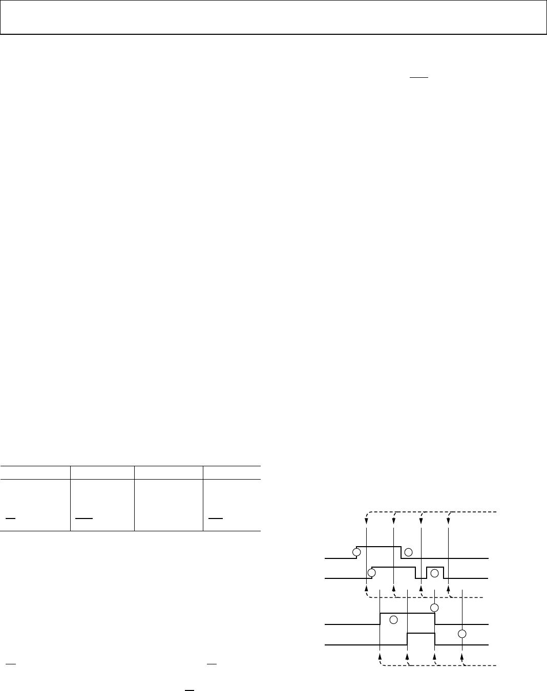
Figure 14 illustrates the behavior of the low speed channels and
the relationship between the codirectional channels.
• Point A: When data is sampled between the input edges of
two low speed data inputs, a very narrow gap between
edges is increased to the width of the output clock.
• Point B: Data edges that occur on codirectional channels
between samples are sampled and simultaneously sent to
the outputs, which synchronizes the data edges between
the two channels at the outputs.
• Point C: Data pulses that are less than the minimum low
speed pulse width may not be transmitted because they
may not be sampled.
INPUT A
OUTPUT A
SAMPLE CLOCK
OUTPUT CLOCK
B
C
INPUT B
OUTPUT B
A
B
C
A
A
12370-014
Figure 14. Slow Channel Timing
Rev. A | Page 18 of 22