Data Sheet ADuM4151/ADuM4152/ADuM4153
The low speed data system is carefully designed so that staggered
data transitions at the inputs become either synchronized or
pushed apart when they are presented at the output. Edge order
is always preserved for as long as the edges are separated by at
least t
VIx SKEW
. In other words, if one edge is leading another at
the input, the order of the edges is not reversed by the isolator.
PRINTED CIRCUIT BOARD (PCB) LAYOUT
The ADuM4151/ADuM4152/ADuM4153 digital isolators
require no external interface circuitry for the logic interfaces.
Power supply bypassing is strongly recommended at both the
V
DD1
and V
DD2
supply pins (see Figure 15). The capacitor value
must be between 0.01 µF and 0.1 µF. The total lead length
between both ends of the capacitor and the input power supply
pin must not exceed 20 mm.
BYPASS < 10mm
V
DD1
GND
1
MCLK
MO
MI
MSS
V
IA
/V
OA
V
IB
/V
OB
V
DD2
GND
2
SCLK
SI
SO
SSS
V
OA
/V
IA
V
IB
/V
OB
V
OC
GND
1
V
IC
GND
2
ADuM4151/
ADuM4152/
ADuM4153
12370-015
Figure 15. Recommended PCB Layout
In applications involving high common-mode transients, it is
important to minimize board coupling across the isolation
barrier. Furthermore, design the PCB layout so that any
coupling that does occur affects all pins equally on a given
component side. Failure to ensure this may cause voltage
differentials between pins that exceed the absolute maximum
ratings of the device, thereby leading to latch-up or permanent
damage.
PROPAGATION DELAY RELATED PARAMETERS
Propagation delay is a parameter that describes the time it takes
a logic signal to propagate through a component. The input to
output propagation delay time for a high to low transition may
differ from the propagation delay time of a low to high
transition.
INPUT
OUTPUT
t
PLH
t
PHL
50%
50%
12370-016
Figure 16. Propagation Delay Parameters
Pulse width distortion is the maximum difference between
these two propagation delay values and an indication of how
accurately the timing of the input signal is preserved.
Channel to channel matching refers to the maximum amount
the propagation delay differs between channels within a single
ADuM4151/ADuM4152/ADuM4153 component.
DC CORRECTNESS AND MAGNETIC FIELD
IMMUNITY
Positive and negative logic transitions at the isolator input cause
narrow (~1 ns) pulses to be sent via the transformer to the decoder.
The decoder is bistable and is, therefore, either set or reset by
the pulses indicating input logic transitions. In the absence of
logic transitions at the input for more than ~1.2 µs, a periodic
set of refresh pulses indicative of the correct input state are sent
via the low speed channel to ensure dc correctness at the output.
If the low speed decoder receives no pulses for more than about
5 µs, the input side is assumed to be unpowered or nonfunctional,
in which case, the isolator output is forced to a high-Z state by
the watchdog timer circuit.
The limitation on the magnetic field immunity of the device is
set by the condition in which induced voltage in the transformer
receiving coil is sufficiently large to either falsely set or reset the
decoder. The following analysis defines such conditions. The
ADuM4151/ADuM4152/ADuM4153 were examined in a 3 V
operating condition because it represents the most susceptible
mode of operation for this product.
The pulses at the transformer output have an amplitude greater
than 1.5 V. The decoder has a sensing threshold of about 1.0 V;
thereby, establishing a 0.5 V margin in which induced voltages
can be tolerated. The voltage induced across the receiving coil is
given by
V = (−dβ/dt)∑πr
n
2
; n = 1, 2, …, N
where:
β is the magnetic flux density.
r
n
is the radius of the n
th
turn in the receiving coil.
N is the number of turns in the receiving coil.
Given the geometry of the receiving coil in the ADuM4151/
ADuM4152/ADuM4153 and an imposed requirement that the
induced voltage be, at most, 50% of the 0.5 V margin at the
decoder, a maximum allowable magnetic field is calculated as
shown in Figure 17.
MAGNETIC FIELD FREQUENCY (Hz)
MAXIMUM ALLOWABLE MAGNETIC FLUX
DENSITY (kgauss)
1k
0.001
100
100M
10
1
0.1
0.01
10k 100k 1M 10M
12370-017
Figure 17. Maximum Allowable External Magnetic Flux Density
Rev. A | Page 19 of 22
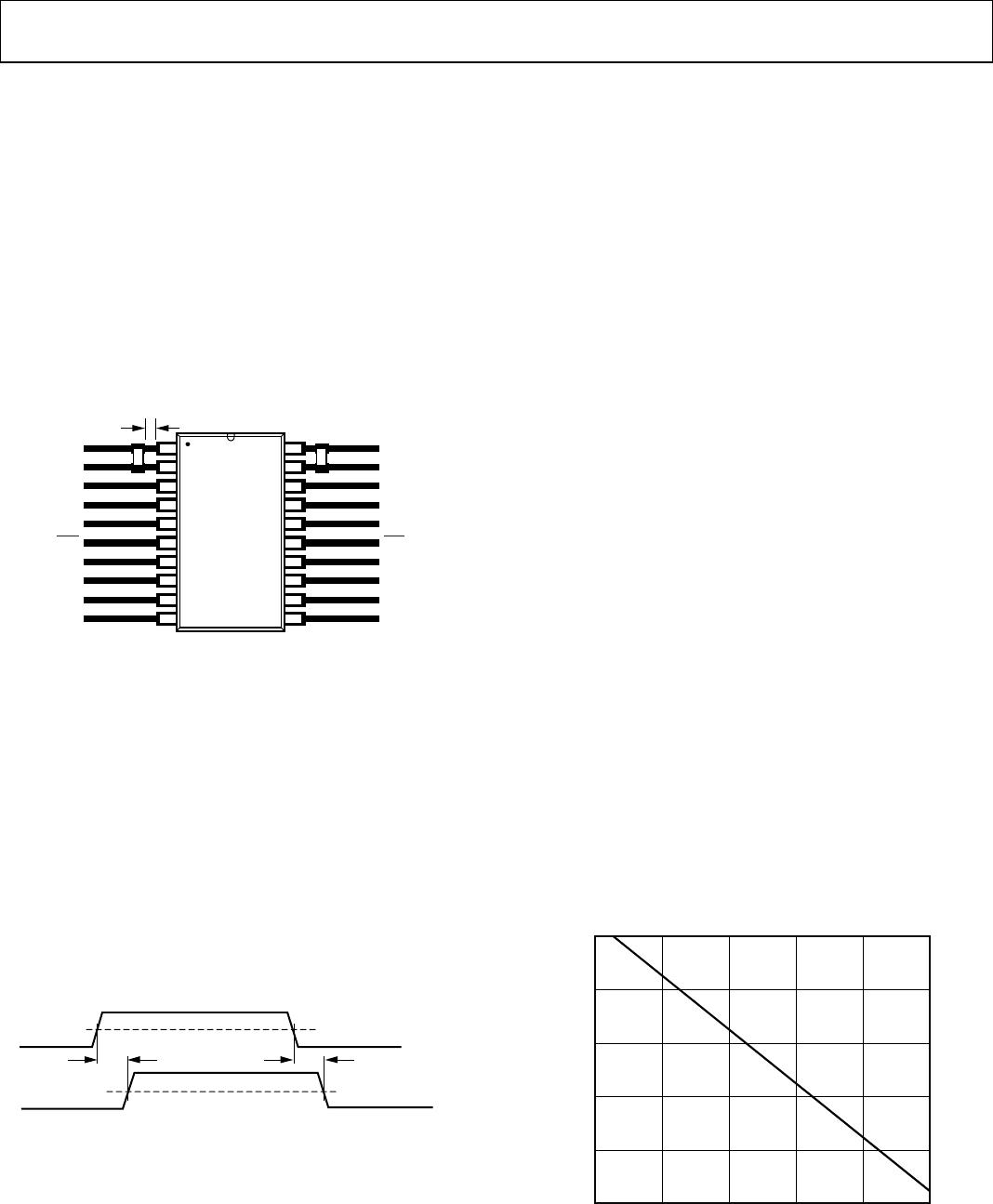
ADuM4151/ADuM4152/ADuM4153 Data Sheet
For example, at a magnetic field frequency of 1 MHz, the
maximum allowable magnetic field of 0.5 kgauss, induces a
voltage of 0.25 V at the receiving coil. This voltage is about 50%
of the sensing threshold and does not cause a faulty output
transition. If such an event occurs, with the worst-case polarity,
during a transmitted pulse, the interference reduces the
received pulse from >1.0 V to 0.75 V. This voltage is still well
above the 0.5 V sensing threshold of the decoder.
The preceding magnetic flux density values correspond to
specific current magnitudes at given distances away from the
ADuM4151/ADuM4152/ADuM4153 transformers. Figure 18
expresses these allowable current magnitudes as a function of
frequency for selected distances. The ADuM4151/ADuM4152/
ADuM4153 are insensitive to external fields. Only extremely
large, high frequency currents, very close to the component are
a concern. For the 1 MHz example noted, placing a 1.2 kA
current 5 mm away from the ADuM4151/ADuM4152/
ADuM4153 affects component operation.
MAGNETIC FIELD FREQUENCY (Hz)
MAXIMUM ALLOWABLE CURRENT (kA)
1000
100
10
1
0.1
0.01
1k 10k 100M100k 1M 10M
DISTANCE = 5mm
DISTANCE = 1m
DISTANCE = 100mm
12370-018
Figure 18. Maximum Allowable Current for Various Current to
ADuM4151/ADuM4152/ADuM4153 Spacings
At combinations of strong magnetic field and high frequency,
any loops formed by the PCB traces may induce sufficiently
large error voltages to trigger the thresholds of succeeding
circuitry. Take care to avoid PCB structures that form loops.
POWER CONSUMPTION
The supply current at a given channel of the ADuM4151/
ADuM4152/ADuM4153 isolators is a function of the supply
voltage, the data rate of the channel, and the output load of the
channel and whether it is a high or low speed channel.
The low speed channels draw a constant quiescent current
caused by the internal ping-pong datapath. The operating
frequency is low enough that the capacitive losses caused by
the recommended capacitive load are negligible compared to
the quiescent current. The explicit calculation for the data rate
is eliminated for simplicity, and the quiescent current for each
side of the isolator due to the low speed channels can be found
in Table 3, Table 6, Table 9, and Table 12 for the particular
operating voltages.
These quiescent currents add to the high speed current as is
shown in the following equations for the total current for each
side of the isolator. Dynamic currents are taken from Table 3
and Table 6 for the respective voltages.
For Side 1, the supply current is given by
I
DD1
= I
DDI(D)
× (f
MCLK
+ f
MO
+ f
MSS
) +
f
MI
× (I
DDO(D)
+ ((0.5 × 10
−3
) × C
L(MI)
× V
DD1
)) + I
DD1(Q)
For Side 2, the supply current is given by
I
DD2
= I
DDI(D)
× f
SO
+
f
SCLK
× (I
DDO(D)
+((0.5 × 10
−3
) × C
L(SCLK)
× V
DD2
)) +
f
SI
× (I
DDO(D)
+((0.5 × 10
−3
) × C
L(SI)
× V
DD2
)) +
f
SSS
× (I
DDO(D)
+((0.5 × 10
−3
) × C
L(
SSS
)
× V
DD2
)) + I
DD2(Q)
where:
I
DDI(D)
, I
DDO(D)
are the input and output dynamic supply currents
per channel (mA/Mbps).
f
x
is the logic signal data rate for the specified channel (Mbps).
C
L(x)
is the load capacitance of the specified output (pF).
V
DDx
is the supply voltage of the side being evaluated (V).
I
DD1(Q)
, I
DD2(Q)
are the specified Side 1 and Side 2 quiescent
supply currents (mA).
Figure 8 and Figure 11 show the typical supply current per
channel as a function of data rate for an input and unloaded
output. Figure 9 and Figure 12 show the total I
DD1
and I
DD2
supply
currents as a function of data rate for the ADuM4151/ADuM4152/
ADuM4153 channel configurations with all high speed channels
running at the same speed and the low speed channels at idle.
INSULATION LIFETIME
All insulation structures eventually break down when subjected
to voltage stress over a sufficiently long period. The rate of
insulation degradation is dependent on the characteristics of the
voltage waveform applied across the insulation as well as the
materials and material interfaces.
Two types of insulation degradation are of primary interest:
breakdown along surfaces exposed to the air and insulation
wear out. Surface breakdown is the phenomenon of surface
tracking and the primary determinant of surface creepage
requirements in system level standards. Insulation wear out is
the phenomenon where charge injection or displacement
currents inside the insulation material cause long-term
insulation degradation.
Rev. A | Page 20 of 22
Data Sheet ADuM4151/ADuM4152/ADuM4153
Rev. A | Page 21 of 22
Surface Tracking
Surface tracking is addressed in electrical safety standards by
setting a minimum surface creepage based on the working
voltage, the environmental conditions, and the properties of the
insulation material. Safety agencies perform characterization
testing on the surface insulation of components that allow the
components to be categorized into different material groups.
Lower material group ratings are more resistant to surface
tracking and, therefore, can provide adequate lifetime with
smaller creepage. The minimum creepage for a given working
voltage and material group is in each system level standard and
is based on the total rms voltage across the isolation, pollution
degree, and material group. The material group and creepage
for the ADuM4151/ADuM4152/ADuM4153 isolators are
detailed in Table 15.
Insulation Wear Out
The lifetime of insulation due to wear out is determined by its
thickness, the material properties, and the voltage stress applied.
It is important to verify that the product lifetime is adequate at
the application working voltage. The working voltage supported
by an isolator for wear out may not be the same as the working
voltage supported for tracking. It is the working voltage
applicable to tracking that is specified in most standards.
Testing and modeling have shown that the primary driver of
long-term degradation is displacement current in the polyimide
insulation causing incremental damage. The stress on the
insulation can be broken down into broad categories, such as
dc stress, which causes very little wear out because there is no
displacement current, and an ac component time varying
voltage stress, which causes wear out.
The ratings in certification documents are usually based on 60 Hz
sinusoidal stress because this stress reflects isolation from line
voltage. However, many practical applications have combinations
of 60 Hz ac and dc across the barrier, as shown in Equation 1.
Because only the ac portion of the stress causes wear out, the
equation can be rearranged to solve for the ac rms voltage, as
shown in Equation 2. For insulation wear out with the
polyimide materials used in this product, the ac rms voltage
determines the product lifetime.
22
DCRMSACRMS
VVV (1)
or
22
DCRMSRMSAC
VVV (2)
where:
V
AC RMS
is the time varying portion of the working voltage.
V
RMS
is the total rms working voltage.
V
DC
is the dc offset of the working voltage.
Calculation and Use of Parameters Example
The following is an example that frequently arises in power
conversion applications. Assume that the line voltage on one
side of the isolation is 240 V ac rms, and a 400 V dc bus voltage
is present on the other side of the isolation barrier. The isolator
material is polyimide. To establish the critical voltages in
determining the creepage clearance and lifetime of a device, see
Figure 19 and the following equations.
ISOLATION VOLTAGE
TIME
V
AC RMS
V
RMS
V
DC
V
PEAK
12370-019
Figure 19. Critical Voltage Example
The working voltage across the barrier from Equation 1 is
22
DCRMSACRMS
VVV
22
400240
RMS
V
V
RMS
= 466 V
The 466 V rms is the working voltage used together with the
material group and pollution degree when looking up the
creepage required by a system standard.
To determine if the lifetime is adequate, obtain the time varying
portion of the working voltage. The ac rms voltage can be
obtained from Equation 2.
22
DCRMSRMSAC
VVV
22
400466
RMSAC
V
V
AC RMS
= 240 V
In this case, the ac rms voltage is simply the line voltage of
240 V rms. This calculation is more relevant when the waveform is
not sinusoidal. The value is compared to the limits for the working
voltage listed in Table 19 for the expected lifetime, less than a 60 Hz
sine wave, and it is well within the limit for a 50-year service life.
Note that the dc working voltage limit in Table 19 is set by the
creepage of the package as specified in IEC 60664-1. This value
may differ for specific system level standards

ADUM4151ARIZ-RL

Mfr. #:
Manufacturer:
Analog Devices Inc.
Description:
Digital Isolators 7 Ch Isolator f or SPI Interface
Lifecycle:
New from this manufacturer.
Delivery:
DHL FedEx Ups TNT EMS
Payment:
T/T Paypal Visa MoneyGram Western Union